Instrument DOI: 10.60551/jb0f-5784
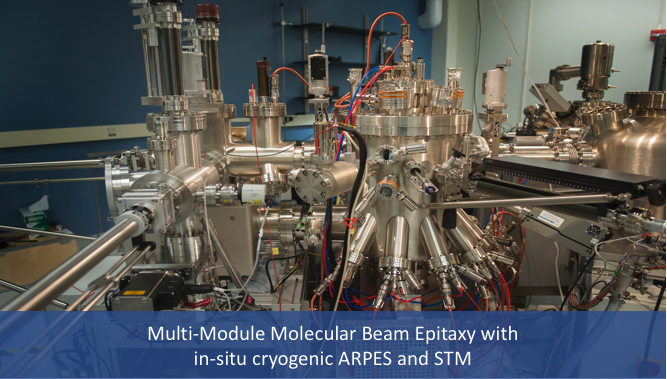
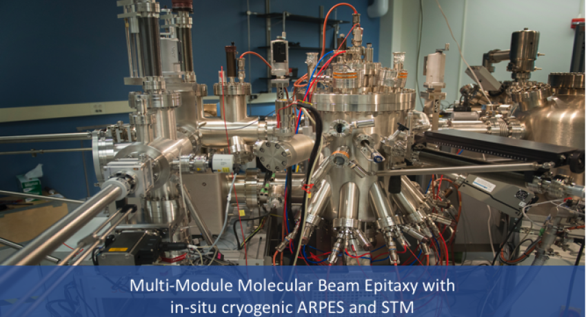
The 2DCC Multi-Module characterization cluster consists of a Molecular Beam Epitaxy (MBE) system connected with in-situ cryogenic Angle Resolved Photoemission Spectroscopy (ARPES) and four-tip Scanning Tunneling Microscopy (STM) tools. Samples can be transferred directly into the characterization tools, without exposing them to atmosphere, allowing the properties of pristine surfaces to be studied. This allows the quickly characterization of sample’s inherent properties and the rapidly development and optimization of new 2D materials and heterostructures. Ports for seven thermal effusion cells and a six pocket e-beam evaporator allow a wide range of materials to be fabricated. In-situ Reflection High Energy Electron Diffraction (RHEED) and spectroscopic ellipsometry allow real-time characterization of films as they grow. The MBE system can grow on up to 2 inch wafers. An adaptor to flag style holders allows growth on up to 1 cm2 substrates that can be transferred in the ARPES and STM modules. The nanoprobe STM features 4 independent tips that can be used for 4-point in-situ electrical transport measurements down to 4.5 K. The integrated scanning electron microscope (SEM) can be used to position each tip independently over chosen features of the sample with a resolution better than 1 micron. Each tip is capable of scanning tunneling measurements although currently only one tip can be used for STM at a time. A small superconducting coil under the sample stage can produce magnetic fields up to 200 gauss. Argon sputtering is available for tip and sample cleaning and preparation.
Instrument DOI: 10.60551/nevd-gb83
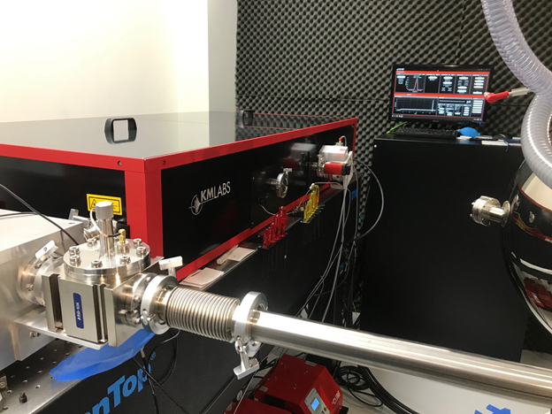
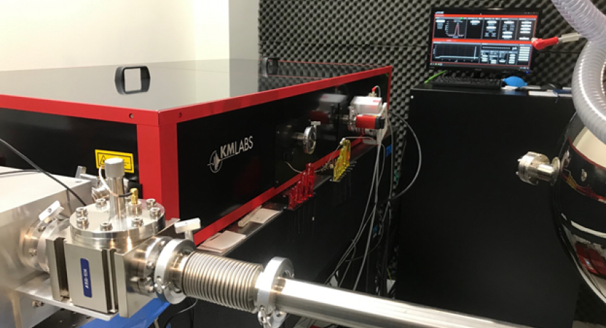
The cryogenic ARPES module features a high intensity helium plasma source and monochromator, allowing energy- and momentum-resolved electronic structure characterization of thin films and single crystals with He 1 (21.22 eV, 23.08 eV), or He 2 (41.81 eV) photon excitation down to a sample temperature below 20 K. The DA-30L spherical analyzer can resolve down to 1.8 meV using a 2 eV pass energy. In addition to the helium light source, the ARPES module is also equipped with a tunable-wavelength Y-Fi laser light source. This system uses high harmonic generation to access four excitation energies in the range of 7.2-10.8 eV with high intensity, while still maintaining energy resolution down to a few meV. Base pressure is 3 x 10⁻¹⁰ mBar.
- 2” diameter substrates, with adaptor for smaller 1 cm2 substrates on Omicron T flag style holders for analysis in ARPES and STM
- Se cracker
- 6 pocket e-beam source for transition metals
- 15kV Reflection High Energy Electron Diffraction (RHEED) system, with kSA 400 RHEED analysis software
- Ellipsometry for real-time film growth monitoring
- Base pressure of 3 x 10⁻¹⁰ mBar
- In-vacuo cryogenic STM with 4 independent probe tips
- In-vacuo cryogenic ARPES (energy resolution 1.8 meV at 2 eV pass energy
- Monochromator with He 1 (21.2 eV) and He 2 (40.8 eV) excitations
- Topological insulators: Bi2Se3, Bi2Te3, (Bi,Sb)2Te3, etc.
- TMDs: MoSe2, MoTe2, NbSe2, WSe2, WTe2, etc…
- FeSe
- Knudsen thermal effusion cells: Bi, Cr, Fe, Sb, and Te
- Cracker cells: Se
- Electron-beam sources: Al, Mo, Nb, Ta, V, and W
For a list of currently available thin film samples click on the link in the left menu.
Yongxi Ou, Wilson Yanez, Run Xiao, Max Stanley, Supriya Ghosh, Boyang Zheng, Wei Jiang, Yu-Sheng Huang, Timothy Pillsbury, Anthony Richardella, Chaoxing Liu, Tony Low, Vincent H. Crespi, K. Andre Mkhoyan, Nitin Samarth, “ZrTe2/CrTe2: an epitaxial van der Waals platform for spintronics,” Nature Communications 13, 2972 (2022). 10.1038/s41467-022-30738-1
L.J. Riddiford, A.J. Grutter, T. Pillsbury, M. Stanley, D.R. Hickey, P. Li, N. Alem, N. Samarth, Y. Suzuki, “Understanding Signatures of Emergent Magnetism in Topological Insulator/Ferrite Bilayers,” Physical Review Letters 128 (12), 126802 (2022). 10.1103/PhysRevLett.128.126802.
Y. Lv, J. Kally, T. Liu, P. Quarterman, T. Pillsbury, B.J. Kirby, A.J. Grutter, P. Sahu, J.A. Borchers, M. Wu, N. Samarth, J.-P. Wang, “Large unidirectional spin Hall and Rashba-Edelstein magnetoresistance in topological insulator/magnetic insulator heterostructures,” Applied Physics Reviews 9 (1), 011406 (2022). 10.1063/5.0073976.
Y. Li, Z. Wang, R. Xiao, Q. Li, K. Wang, A. Richardella, J. Wang, N. Samarth, “Capping layer influence and isotropic in-plane upper critical field of the superconductivity at the FeSe/SrTiO3 interface,” Physical Review Materials 5 (3), 034802 (2021). 10.1103/PhysRevMaterials.5.034802.
W. Yanez, Y. Ou, R. Xiao, J. Koo, J.Y. Held, S. Ghosh, J. Rable, T. Pillsbury, E. Gonzalez Delgado, K. Yang, J. Chamorro, A.J. Grutter, P. Quarterman, A. Richardella, A. Sengupta, T. McQueen, J.A. Borchers, K.A. Mkhoyan, B. Yan, N. Samarth, “Spin and Charge Interconversion in Dirac-Semimetal Thin Films,” Physical Review Applied 16 (5), 054031 (2021). 10.1103/PhysRevApplied.16.054031.
P. Li, J. Ding, S.-L. Zhang, J. Kally, T. Pillsbury, O.G. Heinonen, G. Rimal, C. Bi, A. DeMann, S.B. Field, W. Wang, J. Tang, J.S. Jiang, A. Hoffmann, N. Samarth, M. Wu, “Topological Hall Effect in a Topological Insulator Interfaced with a Magnetic Insulator,” Nano Letters 21 (1), 84- 90 (2021). 10.1021/acs.nanolett.0c03195.
T. Liu, J. Kally, T. Pillsbury, C. Liu, H. Chang, J. Ding, Y. Cheng, M. Hilse, R. Engel-Herbert, A. Richardella, N. Samarth, M. Wu, “Changes of Magnetism in a Magnetic Insulator due to Proximity to a Topological Insulator,” Physical Review Letters 125, 017204 (2020). 10.1103/PhysRevLett.125.017204.
P. Li, J. Kally, S.-L. Zhang, T. Pillsbury, J. Ding, G. Csaba, J. Ding, J.S. Jiang, Y. Liu, R. Sinclair, C. Bi, A. DeMann, G. Rimal, W. Zhang, S.B. Field, J. Tang, W. Wang, O.G. Heinonen, V. Novosad, A. Hoffman, N. Samarth, M. Wu, “Magnetization switching using topological surface states,” Science Advances, 5 (8), eaaw3415 (2019). 10.1126/sciadv.aaw3415