
Instrument DOI: 10.60551/znh3-mj13
 The MOCVD1 system includes a cold wall horizontal metalorganic chemical vapor deposition (MOCVD) reactor from CVD Equipment Corp. with an inductively heated SiC-coated graphite susceptor that can accommodate a single wafer up to 2 inches in diameter at temperatures up to 1000°C. Water circulation through the outer quartz jacket maintains a constant wall temperature. To increase uniformity across the wafer, gas foil rotation of the wafer holder is employed. The reactor loads and unloads through a nitrogen-purged glovebox to minimize exposure to ambient air.
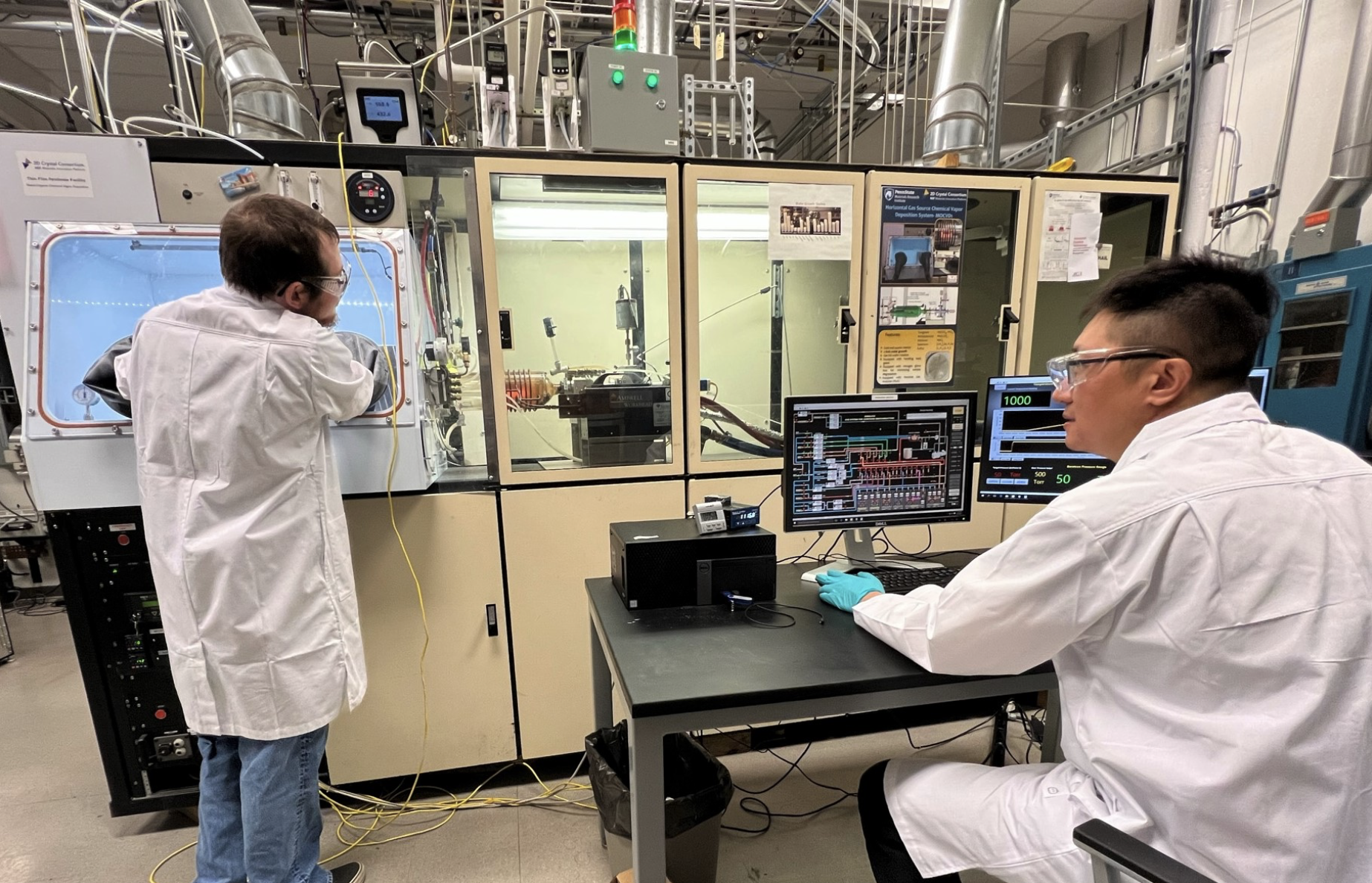
The system includes a welded stainless steel gas panel with metal gasket seal fittings, pneumatic valves, mass flow controllers, pressure controllers, etc. that are operated remotely via custom LabView software. Six bubbler manifolds are available for solid or liquid precursors and gas source lines are available for hydrogen selenide and hydrogen sulfide. A separate connection is available for chloride precursors. Purified hydrogen and nitrogen are available as process gases. A chemically resistant rotary vane pump, capacitance manometer, Pirani gauge, throttle valve controller and additional valves are used to maintain reactor pressures in the range from 10-700 Torr.
The MOCVD reactor and gas panel are housed in a ventilated enclosure. The gas sources are housed within ventilated gas cabinets and are connected to the main system enclosure via double-walled tubing. An exhaust gas scrubber that includes a pyrolysis stage and a packed tower with sodium hydroxide neutralization system is available to treat the reactor effluents to safe limits. A 16-point Honeywell Vertex M chemcassette system is used to monitor for toxic gases at various points on the system and throughout the lab. The MOCVD system is interlocked with the gas detection unit and other sensors to enable safe shutdown in the event of equipment failure.
- Cold wall reactor for 2” diameter substrates with adapter for 10 mm x 10 mm substrates
- Gas foil rotation of wafer holder with argon for uniformity
- Induction heating for graphite susceptor heating
- Dual wavelength fiber optic pyrometer for monitoring substrate temperature
- Toxic gas monitoring by integrated gas detection/exhaust and scrubber/safety system
- Controlled atmosphere sample loading/unloading
- 6 bubblers for liquid/solid sources and 4 gas source lines (H2Se, H2S)
- Wafer scale process developed: WS2, WSe2 and MoS2 monolayers on 2” c-plane sapphire
- Metal Precursors: Mo(CO)6, W(CO)6
- Chalcogen Precursors: H2S, H2Se, Diethyl Sulfide
- Carrier gas: Purified hydrogen or nitrogen
- List of currently available samples
“High-density, localized quantum emitters in strained 2D semiconductors,” G. Kim, H.M. Kim, P. Kumar, M. Rahaman, C.E. Stevens, J. Jeon, K. Jo, K.H. Kim, N. Trainor, H. Zhu, B.H. Sohn, E.A. Stach, J.R. Hendrickson, N.R. Glavin, J. Suh, J.M. Redwing, D. Jariwala, ACS Nano XX,X, XX-XX (2022) https://doi.org/10.1021/acsnano.2c02974.
“Light-matter coupling in large-area van der Waals superlattices,” P. Kumar, J. Lynch, B. Song, H. Ling, F. Barrera, K. Kisslinger, H. Zhang, S.B. Anantharaman, J. Digani, H. Zhu, T.H. Choudhury, C. McAleese, X. Wang, B.R. Conran, O. Whear, M.J. Motala, M. Snure, C. Muratore, J.M. Redwing, N.R. Glavin, E.A. Stach, A.R. Davoyan and D. Jariwala, Nature Nanotechnol. 17, 182-189 (2021). https://doi.org/10.1038/s41565-021-01023-x.
“Wafer-scalable single-layer amorphous molybdenum trioxide,” M. Hasibul Alam, S. Chowdhury, A. Roy, X. Wu, R. Ge, M.A. Rodder, J. Chen, Y. Lu, C. Stern, L. Houben, R. Chrostowski, S.R. Burlison, S. J. Yang, M.I. Serna, A. Dodabalapur, F. Mangolini, D. Navey, J.C. Lee, S.K. Banerjee, J.H. Warner and D. Akinwande, ACS Nano 16, 3, 3756-3767 (2022). https://doi.org/10.1021/acsnano.1c07705.
“Multidimensional imaging reveals mechanisms controlling multimodal label-free biosensing in vertical 2DM-heterostructures,” T. Ignatova, S. Pourianejad, X. Li, K. Schmidt, F. Aryeetey, S. Aravamudhan, S.V. Rotkin, ACS Nano 16, 2, 2598-2607 (2022). https://doi.org/10.1021/acsnano.1c09335.
“Illuminating invisible grain boundaries in coalesced single-orientation WS2 monolayer films,” D. Reifsnyder Hickey, N. Nayir, M. Chubarov, T.H. Choudhury, S. Bachu, L. Miao, Y. Wang, C. Qian, V.H. Crespi, J.M. Redwing, A.C.T. van Duin, N. Alem, Nano Lett. 21, 15, 6487-6495 (2021). https://doi.org/10.1021/acs.nanolett.1c01517.
“Wafer-scale epitaxial growth of unidirectional WS2 monolayers on sapphire,” M. Chubarov, T.H Choudhury, D. Reifsnyder Hickey, S. Bachu, T. Zhang, A. Sebastian, A. Bansal, H. Zhu, N. Trainor, S. Das, M. Terrones, N. Alem and J.M. Redwing, ACS Nano 15, 2, 2532-2541(2021). https://doi.org/10.1021/acsnano.0c06750.
“Benchmarking monolayer MoS and WS2 field-effect transistors,” A. Sebastian, R. Pendurthi, T.H. Choudhury, J.M. Redwing and S. Das, Nature Communications 12, 1, 1-12 (2021). https://doi.org/10.1038/s41467-020-20732-w.
“Monolayer MoS2 on sapphire: an azimuthal reflection high-energy electron diffraction perspective,” Y. Xiang, X. Sun, L. Valdman, F. Zhang, T.H. Choudhury, M. Chubarov, J.A. Robinson, J.M. Redwing, M. Terrones, Y. Ma, L. Gao, M.A. Washington, T.H. Lu and G.C. Wang, 2D Materials 8, 2 025003 (2020). https://doi.org/10.1088/2053-1583/abc905.
“A low power biomimetic collision detector based on an in-memory molybdenum disulfide photodetector,” D. Jayachandran, A. Oberoi, A. Sebastian, T.H. Choudhury, B. Shankar, J.M. Redwing and S. Das, Nature Electronics 3 646-655 (2020). https://doi.org/10.1038/s41928-020-00466-9.
"Multi-scale modeling of gas phase reactions in metal-organic chemical vapor deposition growth of WSe2,” Y. Xuan, A. Jain, S. Zafar, R. Lotfi, N. Nayir, Y. Wang, T.H. Choudhury, S. Wright, J. Feraca, L. Rosenbaum, J.M. Redwing, V. Crespi and A. van Duin, J. Crystal Growth 527, 125247 (2019). https://doi.org/10.1016/j.jcrysgro.2019.125247