
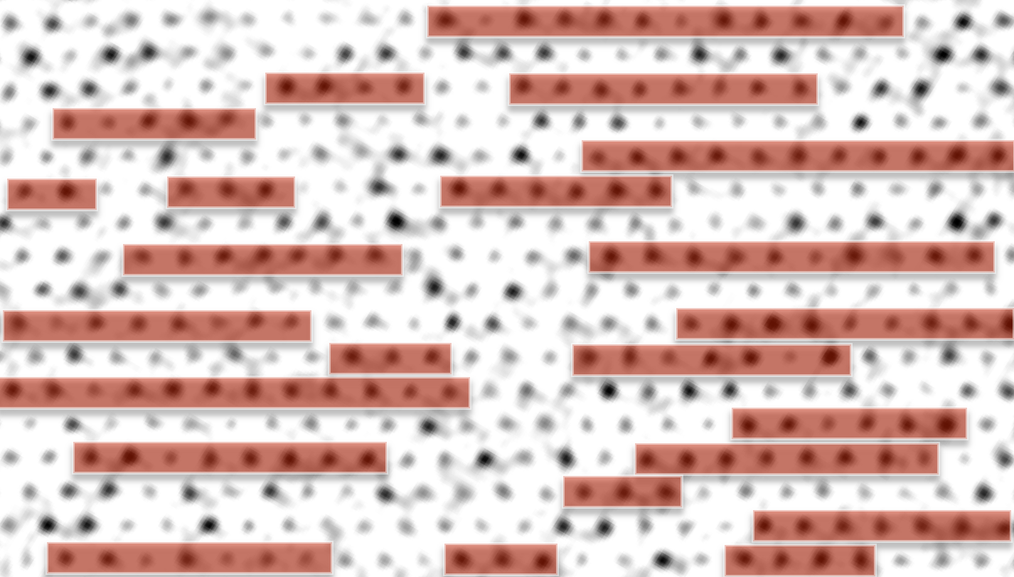
Transmission electron microscopy image of the distribution of Mo and W atoms within a 2D layer of a molybdenum/tungsten disulfide semiconductor alloy. Red bars mark the locations of stripes of tungsten.
What Has Been Achieved:
A new mechanism to control the placement of metal atoms within 2D chalcogenide materials, to form ordered stripes.
Importance of Achievement:
Control of atomic order is key to optimizing materials properties of all kinds, and in this case particularly properties that are sensitive to the masses of the atoms, or their different electronic structure. In 3D semiconductors, the ordering of different layers of material into so-called heterostructures was key to developing device applications of various kinds. The analog in 2D would be control of 1D stripes of material within the 2D layer. This is a first demonstration of such a degree of control.
Unique Features of the MIP That Enabled Project:
The close collaboration between theory and experiment in the 2DCC-MIP, and the focus of the program on overcoming key challenges in 2D synthesis coupled to advanced characterization, were central to this advance.
Credits/Names: A. Azizi, Y. Wang, Z. Lin, K. Wang, A.L. Elias, M. Terrones, V.H. Crespi, and N. Alem, “Spontaneous Formation of Atomically Thin Stripes in Transition Metal Dichalcogenide Monolayers,” Nano Lett. 2016, 16 (11), 6982−6987, DOI: 10.1021/acs.nanolett.6b03075
Download PDF Version: Atomically Thin Stripes In Monolayer Sheets.pdf
Year of Research Highlight: 2016