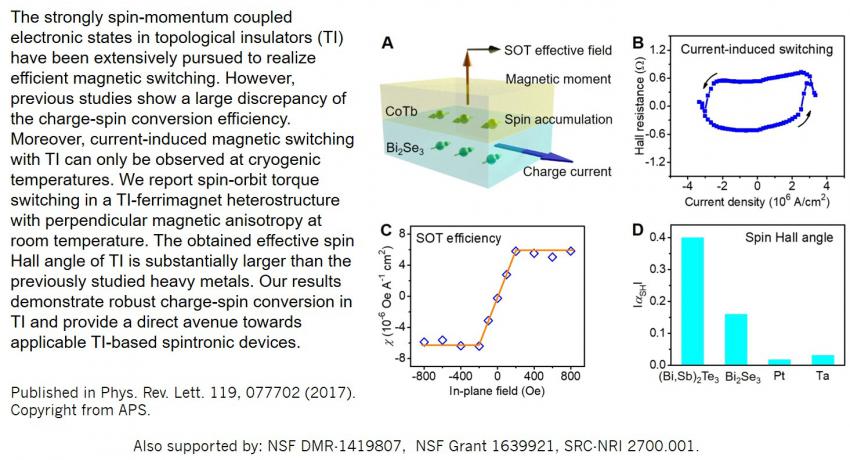
What Has Been Achieved:
What Has Been Achieved:
What Has Been Achieved:
What Has Been Achieved:
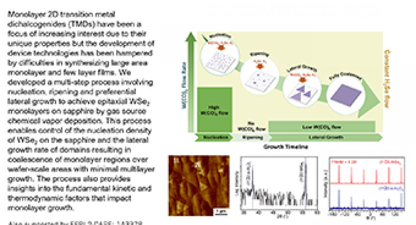
A multi-step process was developed to achieve large…
What Has Been Achieved:
The 2DCC-MIP is funded by NSF cooperative agreement DMR-2039351.
MRI is not responsible for the content of external sites. Registration may be required for some sites.
General inquiries: mri-info@psu.edu | Website inquiries: mri-web@psu.edu