
Instrument DOI: 10.60551/gqq8-yj90
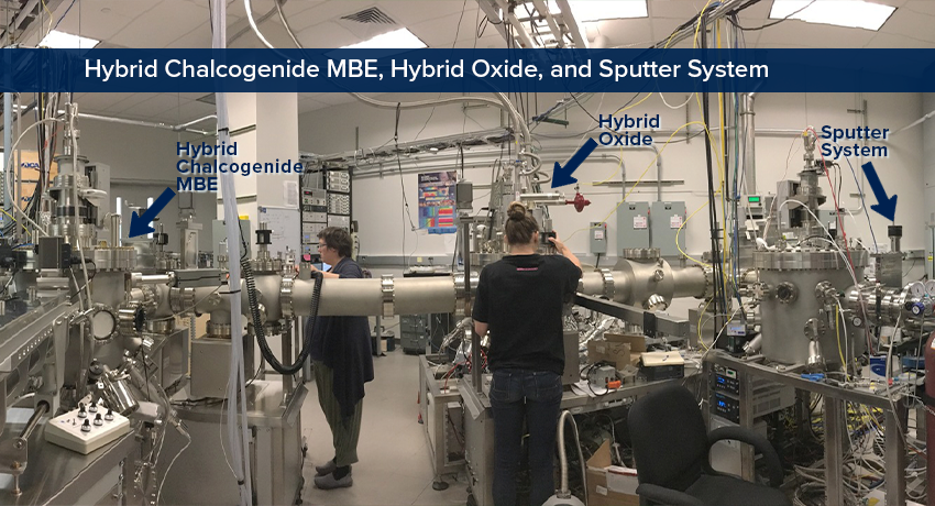
The 2DCC Hybrid Chalcogenide Molecular Beam Epitaxial (MBE) system is an MBE system dedicated to the growth of chalcogenide thin films. The hybrid MBE approach enables the synthesis of chalcogenide materials containing refractory metallic components through the addition of a low temperature cell, allowing the use of solid state precursors with higher vapor pressures than pure refractory metals. MBE2 is equipped with a selenium cracker cell, allowing users to choose the specific Se species needed for their material. To guarantee the highest degree of control down to a single layer and excellent reproducibility the chalcogenide MBE reactor is equipped with a series of state of the art in-situ monitoring capabilities, such as reflection high energy electron diffraction, ion gauge beam flux monitor, residual gas analyzer, heated quartz crystal monitor, and a spectroscopic ellipsometer. The hybrid chalcogenide MBE can handle wafers as large as 3 inches and as small as 1 cm x 1 cm, with the ability to grow multiple samples simultaneously. The chalcogenide MBE reactor is connected via a UHV transfer line to an oxide MBE reactor and shares a lab with a III-V MBE system. The in-vacuo transfer to the oxide system and the glove bag transfer to the III-V system enables the integration of chemically dissimilar materials, such as growth of chalcogenide films on oxide thin films or on III-V heterostructures (e.g. back gates). In-vacuo sample exchange using a vacuum suitcase allows samples grown in MBE2 to be characterized in the 2DCC MIP thin film characterization cluster located in Davey Laboratory at Penn State University, various characterization tools located in the Materials Characterization Lab at Penn State, as well as other 2DCC tools. This enables surface sensitive characterization techniques, such as angle resolved photoelectron emission spectroscopy, scanning tunneling microscopy, and transport measurements to be done without air exposure.
- Up to 3” diameter substrates, adapter for (10x10)mm substrates, adapter for samples on Omicron T flag style holders
- Ultra-high vacuum shuttle for post growth characterization with up to 3 flag style holder sample storage capacity, base pressure 5×10⁻¹⁰ Torr, equipped with a NexTorr pump keeping this vacuum for weeks without power supply
- Reflection high energy electron diffraction (RHEED) system 15kV, with RHEED analysis software kSA 400 version 5.50
- Spectroscopic ellipsometer, spectral range of 210-1690nm
- Residual gas analyzer for real-time background gas analysis
- Fully automated ion gauge beam flux monitor
- Fully automated heated quartz crystal monitor (room temperature to 500ºC)
- Pyrometer for remote sample temperature measurements (in conjunction with in-situ spectroscopic ellipsometer)
- Chalcogenide reactor base pressure of 1×10⁻¹⁰ Torr
- Radio frequency plasma source to be used for oxygen, argon and nitrogen
- 8 effusion cells (3 low temperature cells, 2 high temperature cells, 2 dual temperature cells, 1 cracker cell)
- 4-pocket electron-beam evaporator source for high refractory metals with long throw distance to minimize thermal load on sample during e-beam operation
- Adapter to a 4-line gas-injector inlet system of metal-organic precursors
- All components are gate valve isolated to maximize uptime and allow maintenance during operation
- Solid source: Se, In, Bi, Fe, Te, Sn, Eu, Ga
- Electron-beam source: Pt, Si, Ge, Pd
“Measuring and Then Eliminating Twin Domains in SnSe Thin Films Using Fast Optical Metrology and Molecular Beam Epitaxy,” W. Mortelmans, M. Hilse, Q. Song, S. Soon Jo, K. Ye, D. Liu, N. Samarth, R. Jaramillo, ACS Nano 16 , 9472-9478 (2022), https://doi.org/10.1021/acsnano.2c02459
“Probing the growth quality of molecular beam epitaxy-grown Bi2Se3 films via in-situ Spectroscopic ellipsometry,” A. Bai, M. Hilse, P. D. Patil, R. Engel-Herbert, F. Peiris, J. Cryst. Growth 591, 126714 (2022), https://doi.org/10.1016/j.jcrysgro.2022.126714
“Molecular beam epitaxy of PtSe2 using a co-deposition approach,” M. Hilse, K. Wang, R. Engel-Herbert, 2D Mater. 9, 025029 (2022), https://iopscience.iop.org/article/10.1088/2053-1583/ac606f
“Substrate Modification during Chemical Vapor Deposition of hBN on Sapphire,” A. Bansal, M. Hilse, B. Huet, K. Wang, A. Kozhakhmetov, J. Hyun Kim, S. Bachu, N. Alem, R. Collazo, J. A. Robinson, R. Engel-Herbert, J. M. Redwing, ACS Appl. Mater. Interfaces 13, 45, 54516-54526 (2021), https://pubs.acs.org/doi/10.1021/acsami.1c14591
“Spectroscopic ellipsometry as an in-situ monitoring tool for Bi2Se3 films grown by molecular beam epitaxy,” M. Hilse, X. Wang, P. Killea, F. Peiris, R. Engel-Herbert, J. Cryst. Growth 566-567, 126177 (2021), https://doi.org/10.1016/j.jcrysgro.2021.126177
“Sticking coefficients of selenium and tellurium,” D. S. H. Liu, M. Hilse, R. Engel-Herbert, J. Vac. Sci. Technol. A 39, 023413 (2021), https://avs.scitation.org/doi/10.1116/6.0000736
“Changes of Magnetism in a Magnetic Insulator due to Proximity to a Topological Insulator,” T. Liu, J. Kally, T. Pillsbury, C. Liu, H. Chang, J. Ding, Y. Cheng, M. Hilse, R. Engel-Herbert, A. Richardella, N. Samarth, M. Wu, Phys. Rev. Lett. 125, 1, 017204 (2020), https://doi.org/10.1103/PhysRevLett.125.017204
“Growth of ultrathin Pt layers and selenization into PtSe2 by molecular beam epitaxy,” M. Hilse, R. Engel-Herbert, 2D Mater. 7, 4, 045013 (2020), https://iopscience.iop.org/article/10.1088/2053-1583/ab9f91
“Large-scale Fabrication of Submicron-gate-length MOSFETs with a Trilayer PtSe2 Channel Grown by Molecular Beam Epitaxy,” K. Xiong, M. Hilse, L. Li, A. Göritz, M. Wietstruck, M. Kaynak, R. Engel-Herbert, A. Madjar, J. C. M. Hwang, IEEE Transaction on Electron Devices 67, 3, 796-801, (2020), https://doi.org/10.1109/TED.2020.2966434