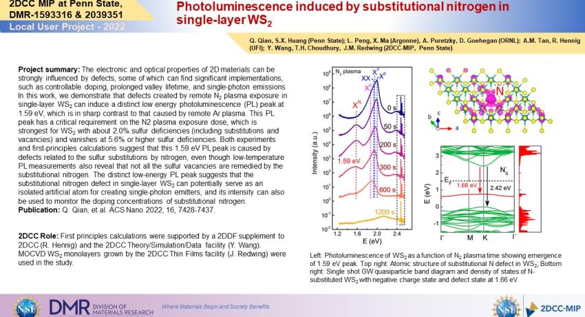
Project summary: The electronic and optical properties of 2D materials can be strongly influenced by defects, some of which can find significant implementations, such as controllable doping, prolonged valley lifetime, and single-photon emissions. In this work, we demonstrate that defects created by remote N2 plasma exposure in single-layer WS2 can induce a distinct low energy photoluminescence (PL) peak at 1.59 eV, which is in sharp contrast to that caused by remote Ar plasma. This PL peak has a critical requirement on the N2 plasma exposure dose, which is strongest for WS2 with about 2.0% sulfur deficiencies (including substitutions and vacancies) and vanishes at 5.6% or higher sulfur deficiencies. Both experiments and first-principles calculations suggest that this 1.59 eV PL peak is caused by defects related to the sulfur substitutions by nitrogen, even though low-temperature PL measurements also reveal that not all the sulfur vacancies are remedied by the substitutional nitrogen. The distinct low-energy PL peak suggests that the substitutional nitrogen defect in single-layer WS2 can potentially serve as an isolated artificial atom for creating single-photon emitters, and its intensity can also be used to monitor the doping concentrations of substitutional nitrogen.
Publication: Q. Qian, et al. ACS Nano 2022, 16, 7428-7437.
2DCC Role: First principles calculations were supported by a 2DDF supplement to 2DCC (R. Hennig) and the 2DCC Theory/Simulation/Data facility (Y. Wang). MOCVD WS2 monolayers grown by the 2DCC Thin Films facility (J. Redwing) were used in the study.
