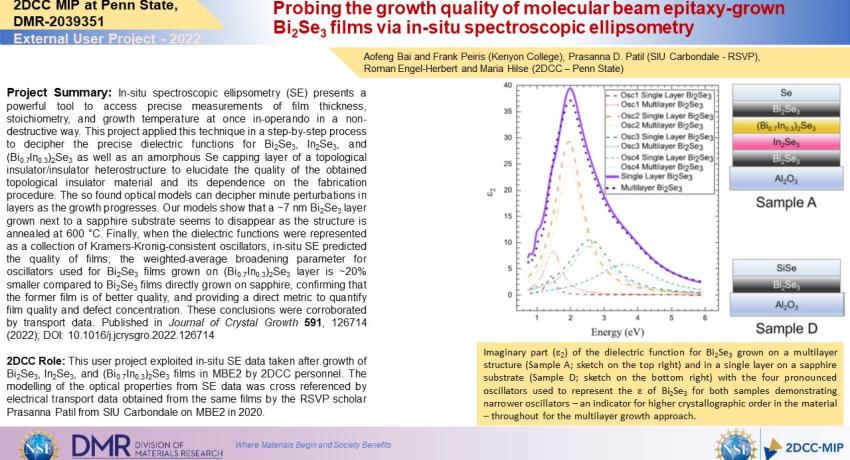
Project Summary: In-situ spectroscopic ellipsometry (SE) presents a powerful tool to access precise measurements of film thickness, stoichiometry, and growth temperature at once in-operando in a non-destructive way. This project applied this technique in a step-by-step process to decipher the precise dielectric functions for Bi2Se3, In2Se3, and (Bi0.7In0.3)2Se3 as well as an amorphous Se capping layer of a topological insulator/insulator heterostructure to elucidate the quality of the obtained topological insulator material and its dependence on the fabrication procedure. The so found optical models can decipher minute perturbations in layers as the growth progresses. Our models show that a ~7 nm Bi2Se3 layer grown next to a sapphire substrate seems to disappear as the structure is annealed at 600 °C. Finally, when the dielectric functions were represented as a collection of Kramers-Kronig-consistent oscillators, in-situ SE predicted the quality of films; the weighted-average broadening parameter for oscillators used for Bi2Se3 films grown on (Bi0.7In0.3)2Se3 layer is ~20% smaller compared to Bi2Se3 films directly grown on sapphire, confirming that the former film is of better quality, and providing a direct metric to quantify film quality and defect concentration. These conclusions were corroborated by transport data. Published in Journal of Crystal Growth 591, 126714 (2022); DOI: 10.1016/j.jcrysgro.2022.126714
2DCC Role: This user project exploited in-situ SE data taken after growth of Bi2Se3, In2Se3, and (Bi0.7In0.3)2Se3 films in MBE2 by 2DCC personnel. The modelling of the optical properties from SE data was cross referenced by electrical transport data obtained from the same films by the RSVP scholar Prasanna Patil from SIU Carbondale on MBE2 in 2020.
What Has Been Achieved: This paper reported for the first time the real-time in-operando observation of the degree of crystallographic ordering in a Bi2Se3 film that corresponded to ex-situ assessment of film quality through electronic transport measurements.
Importance of the Achievement: A precise understanding of the quality of crystal properties of topological insulators and their improvement is crucial to advance the field of quantum materials to harvest their properties in future applications.
Unique Feature(s) of the MIP that Enabled this Achievement: The 2DCC has established growth procedures for quantum materials and topological and trivial band structure materials such as Bi2Se3 and In2Se3 on MBE2. The in-situ SE setup on MBE2 proved instrumental for this study. The RSVP scholar fund from 2DCC further enabled a comprehensive study of the electronic transport characteristics of those materials which contributed an important piece to this study.
(If Applicable) Publication:
Aofeng Bai, Maria Hilse, Prasanna D. Patil, Roman Engel-Herbert, Frank Peiris Journal of Crystal Growth 591, 126714 (2022); DOI: 10.1016/j.jcrysgro.2022.126714
Acknowledgements: The work at Kenyon College was supported by the NSF grant DMR-2004812. This work at The Pennsylvania State University was facilitated by the Two-Dimensional Crystal Consortium – Materials Innovation Platform (2DCC-MIP) at The Pennsylvania State University, which is supported by NSF cooperative Agreement No. DMR-2039351. P.D.P. acknowledges the support provided by the Graduate School, Southern Illinois University Carbondale, through the Doctoral Fellowship and 2DCC-MIP, the Pennsylvania State University through Resident Scholar Visitor Program (RSVP).
