
 |
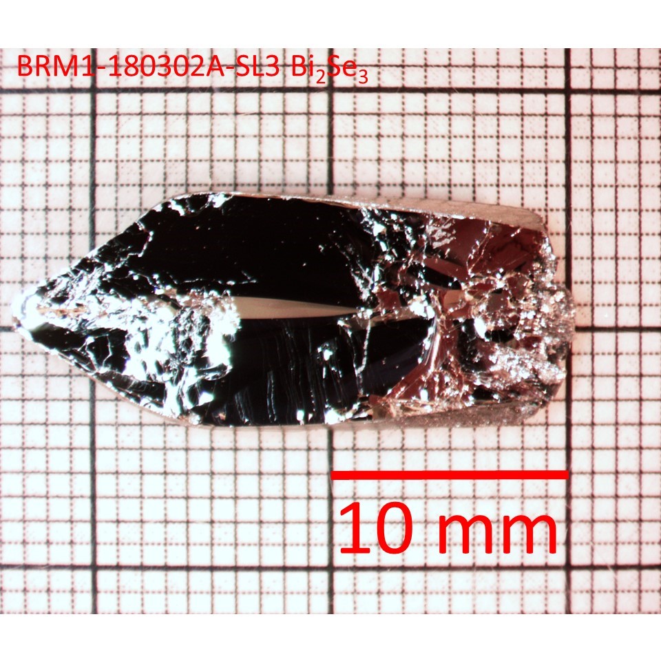
Bi2Se3 Bi2Se3 is a well-known topological insulator. This system has rhombohedral layered crystal structure with quintuple layers (QLs) ordered in a Se-Bi-Se-Bi-Se sequence along the c-axis. The QLs weakly interact through the van der Waals forces and therefore the materials cleave easily between QLs. The typical n-type charge carrier density and Hall mobility are about 1018 cm-3 and 700 cm2/Vs at room temperature. |
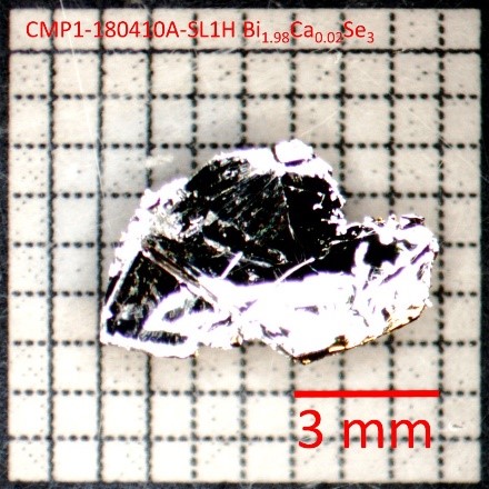 |
Bi1.98Ca0.02Se3 Bi2Se3 is a topological insulator with n-type carrier charge due to selenium self-vacancies. p-type Bi2Se3 single crystal is synthesized by substituting calcium on bismuth site to compensate the electrons created by the selenium vacancies. The typical charge carrier density and Hall mobility are about 1018 cm-3 and 2000 cm2/Vs at 2K, respectively. The Fermi level of the system located in the bulk bandgap, suggested from the Scanning Tunneling Spectroscopy (STS) spectra, the system suitable for the topological surface states study. |
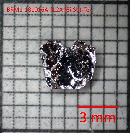 |
(Bi,Sb)2Te3 Bi2Te3 is one of the good thermoelectric materials and has been commercialized for a wide range of applications in power generation and refrigeration. By alloying the Bi2Te3 and Sb2Te3, it allows us to fine-tune the carrier density as well as the reduction in lattice thermal conductivity. |
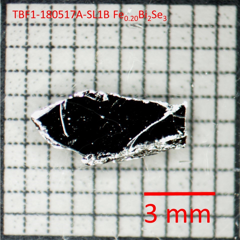 |
Fe-doped Bi2Se3 Time-reversal symmetry (TRS) can be broken when a magnetic order is introduced into topological insulators and resulting the non-trivial topological surface drives into a new massive Dirac fermion state. By intercalating iron into Bi2Se3 quintuple layers, the magnetic ground state of the system is antifferomagentic with TN = 100K. However, this system is also a metamagentic system, where the magnetic properties of the system can be driven into ferromagnetic by external magnetic field, Hc ~ 400 Oe. The typical n-type charge carrier density and Hall mobility are about 1019 cm-3 and 1700 cm2/Vs at 2K. |
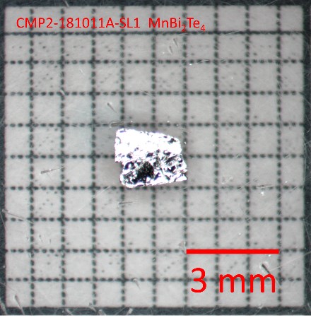 |
MnBi2Te4 MnBi2Te4 has recently been established as the first intrinsic antiferromagnetic (AFM) topological insulator (TI) with TN = 25K. Several exotic properties, such as quantum anomalous Hall effect (QAHE), axion insulator, and layered Hall effect have been experimentally observed in its 2D limit. |
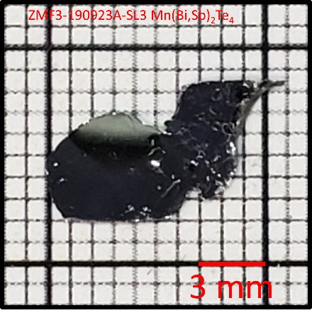 |
Mn(Bi1-xSbx)2Te4 The as-grown MnBi2Te4 is heavily electron-doped possible due to non-stoichiometry or antisite defects. By partially substituting Sb for Bi, its Fermi level not only can be tuned from the bulk conduction band (electron-doped) to the bulk valence band (hole-doped) but also its carrier mobility is dramatically enhanced. It makes the system suitable to realize the proposed topological state, such as idea Weyl semimetal. We capable of growing Mn(Bi1-xSbx)2Te4 from x = 0 to x = 1.0 |
 |
MnBi4Te7 MnBi4Te7 is an antiferromagnetic topological insulator (TN = 13K), with the building block of septuple layer MnBi2Te4 and a quintuple layer of Bi2Te3. Due to the weak interlayer magnetic coupling as compared to MnBi2Te4, an antiferromagnetic with a small saturation field is achieved. |
 |
Mn(Bi1-xSbx)6Te10 Via controlling the parameters of growth condition, we can realize both FM state and AFM state in MnBi6Te10, without any doping for the first time. The ferromagnetic transition temperature is TC ~ 13K. Similar to MnBi4Te7, MnBi6Te10 consists of the building block of septuple layer MnBi2Te4 and two quintuple layer of Bi2Te3. Theory predicts that a variety of exotic topological states, such as quantum anomalous Hall insualtor, Mobius insulator, high order topological state, quantum spin Hall effect, and hinged quantum spin hall effect can be realized. We capable of growing Mn(Bi1-xSbx)6Te10 from x = 0 to x = 0.3 |
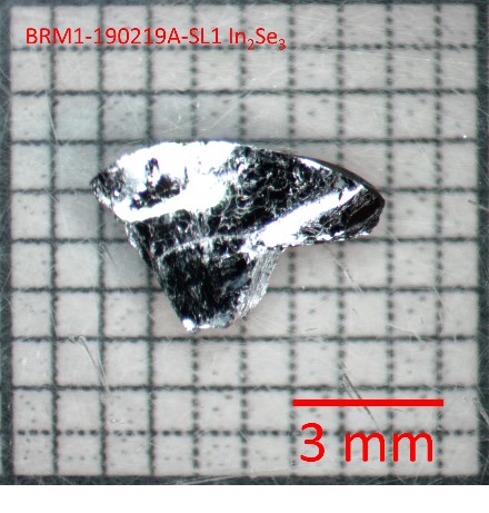 |
α-In2Se3 α-In2Se3 is a layered transition metal chalcogenide featuring a van de Waals interlayer coupling and an energy gap of 1.4 eV. This material was predicted to be a ferroelectric material in bulk.
|
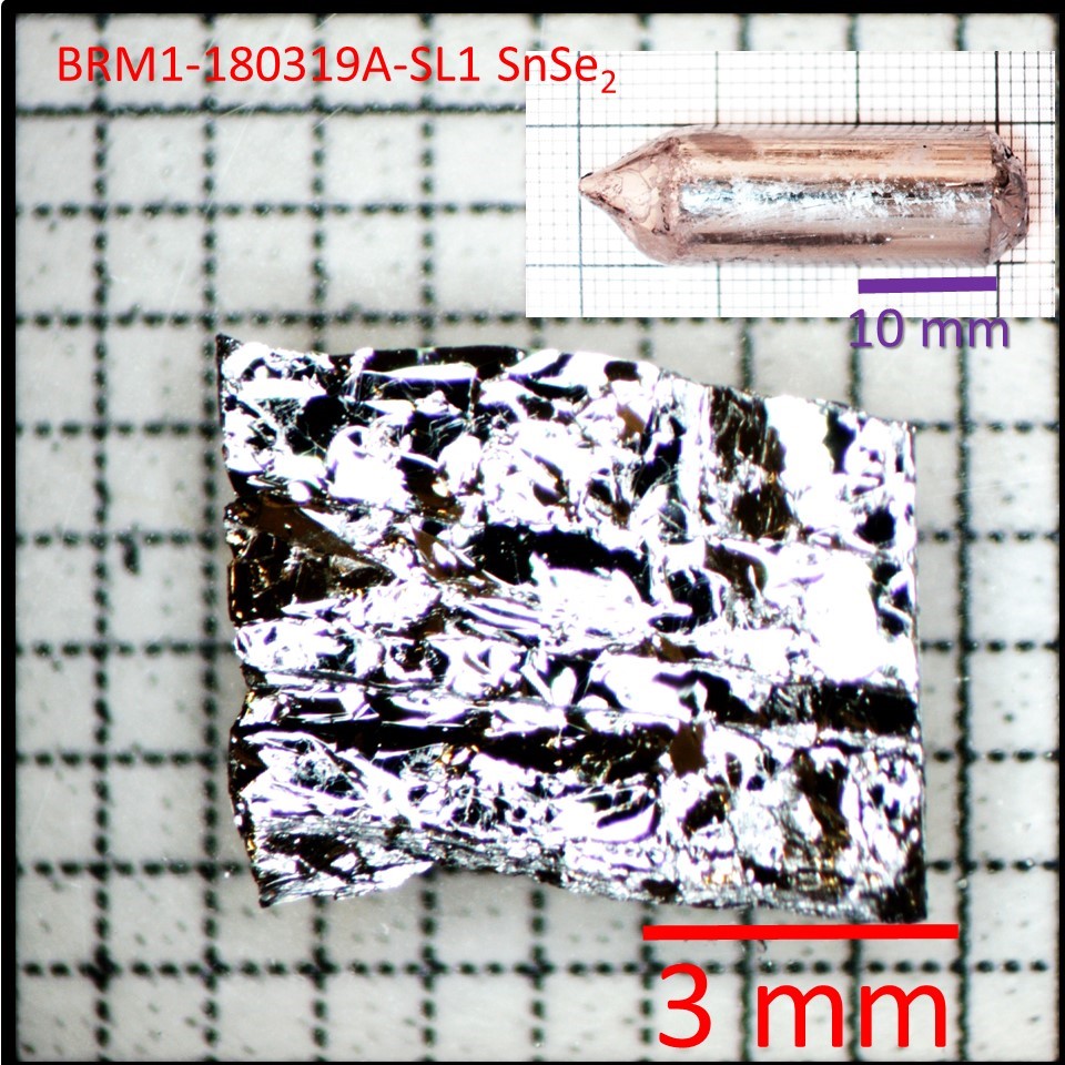 |
SnSe2 SnSe is a transition metal dichalcogenide. The system can be exfoliated into thin 2D layers due to the weakly-bounded layered structure. The typical n-type charge carrier density and Hall mobility are about 1017 cm-3 and 30 cm2/Vs at room temperature. |
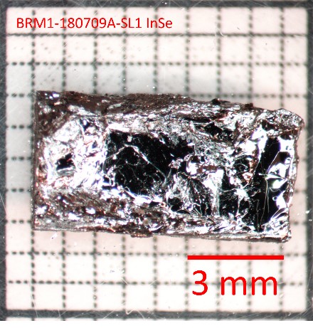 |
InSe InSe is a mono-chalcogenides layered compound. It receives great interest due to the exceptional properties, such as high electron mobility, tunable absorption, and extremely strong photoresponse. XRD pattern suggests the crystal is in β-phase.
|
|
|
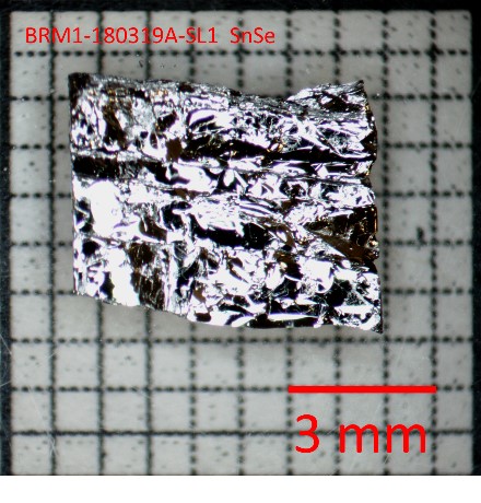
SnSe SnSe is a semiconductor with a bulk indirect bandgap of 0.9eV. Due to its low thermal conductivity as well as electrical conductivity, it is one of the most efficient thermoelectric materials. |
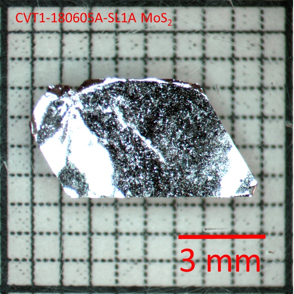 |
MoS2 MoS2 is a well-known transition metal dichalcogenide and recently experimental demonstrates the gate-induced superconductivity in exfoliated MoS2 multilayers. The typical charge carrier density for MoS2 sample is about 1015. |
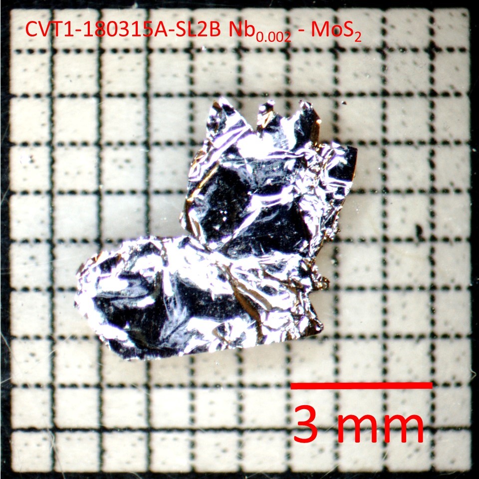 |
Nb-doped MoS2 MoS2 is a well-known transition metal dichalcogenide and recently experimental demonstrates the gate-induced superconductivity in exfoliated MoS2 multilayers. p-type MoS2 can be synthesized by niobium doping. The typical p-type charge carrier density and Hall mobility of our Nb-doped MoS2 sample are about 1018 to 1019 cm-3 and 15 cm2/Vs at room temperature. |
 |
MoSe2 MoSe2 is a semiconductor with a bulk indirect bandgap of 1.1 eV.
|
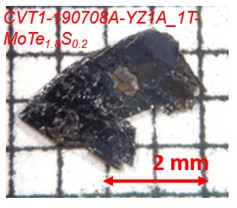 |
1T-MoTe1.8S0.2 1T-MoTe1.8S0.2 is a superconductors with Tc~1.3K |
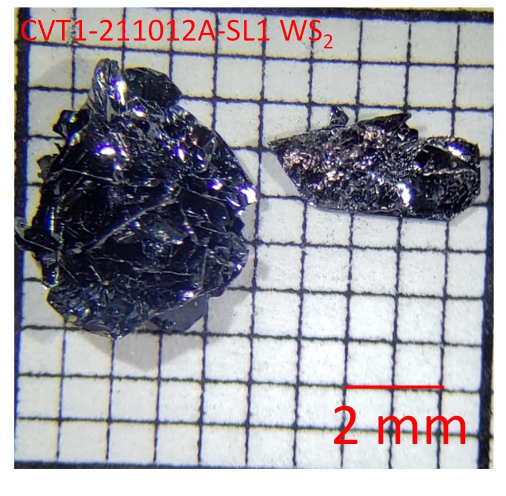 |
WS2 Bulk WS2 forms dark gray hexagonal crystals with a layered structure. Like the closely related MoS2, WS2 is a semiconductor with a bulk indirect bandgap of ~1.35eV . |
 |
WSe2 WSe2 is a semiconductor with a bulk indirect bandgap of ~1.2eV. |
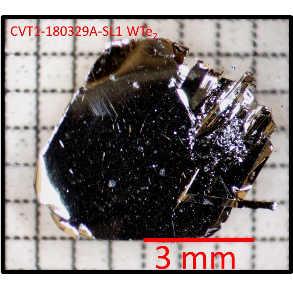 |
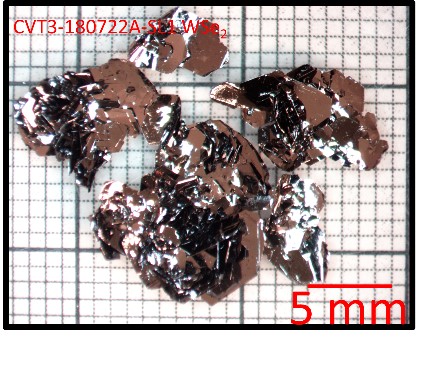
1T’ and 1Td-WTe2 WTe2 is a well-known transition metal dichalcogenide. It is also a type-II Weyl semimetal. The typical n-type charge carrier density and Hall mobility are about 1020 cm-3 and 40 cm2/Vs at room temperature. |
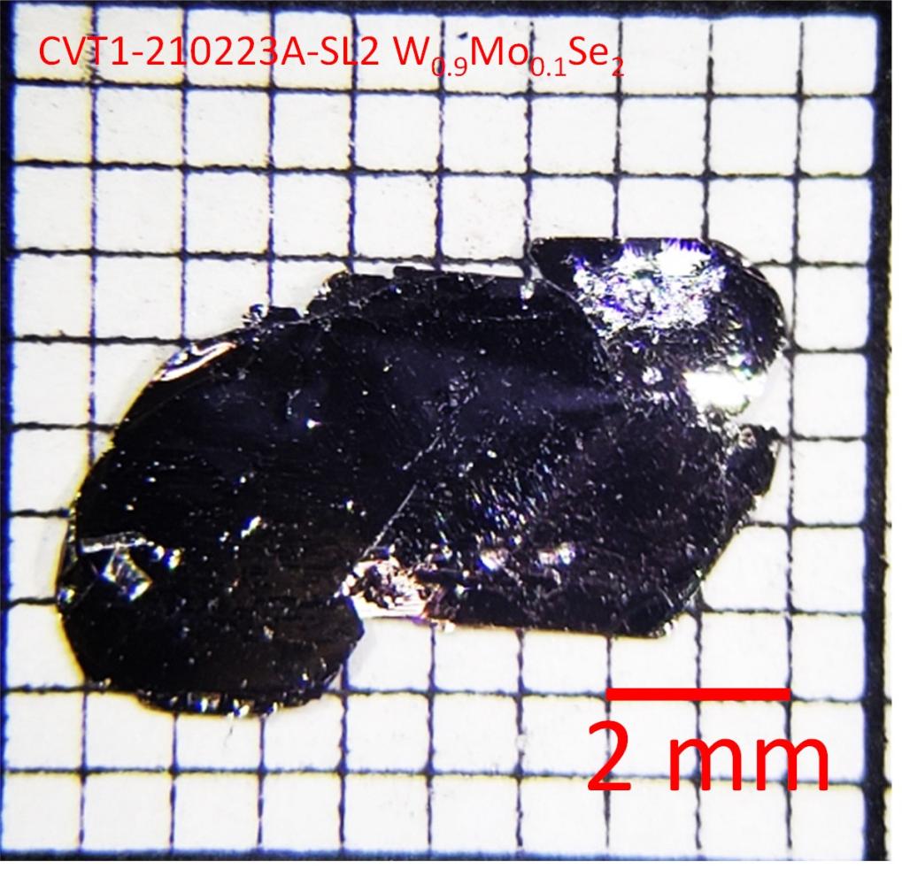 |
(W1-xMox)Se2 (W1-xMox)Se2 is a semiconductor. The currently available alloy is rich in Tungsten with 10% Mo.
|
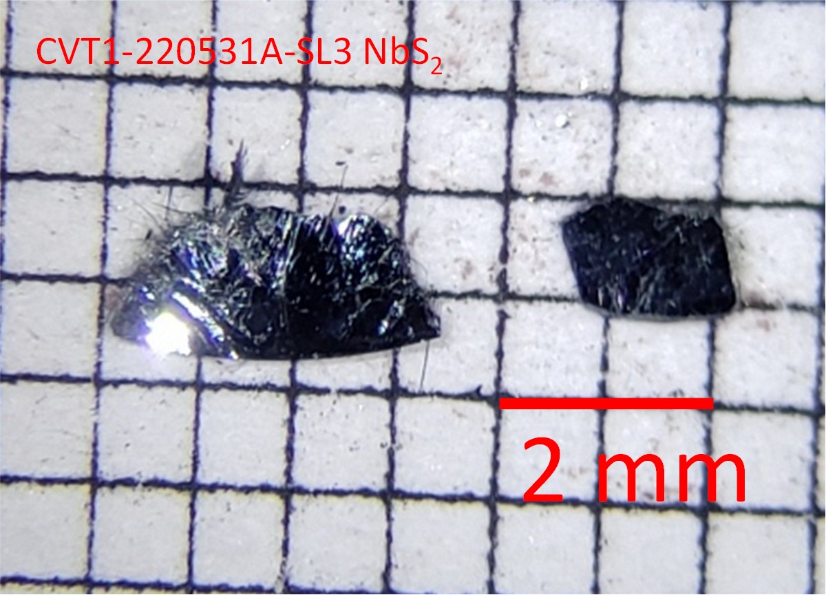 |
NbS2 NbS2 is a metal with the emergence of a superconducting state at Tc ~ 6 K and a charge density waves (CDW) system.
|
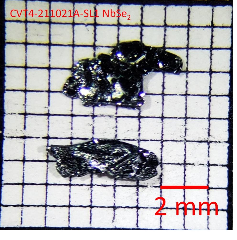 |
NbSe2 NbSe2 is a metal with the emergence of a supercoucting state at Tc ~ 7.2 K and a charge density waves (CDW) state at Tcdw ~ 33 K. |
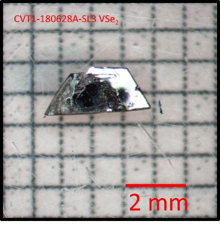 |
VSe2 VSe2 has a metallic behavior in the resistivity measurement with a charge density wave below 110K. This material receives great interest due to the observation of ferromagnetic ordered in monolayer at room temperature. |
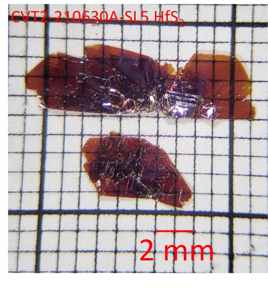 |
HfS2 HS2 is a semiconductor with a bulk indirect bandgap of ~2eV. |
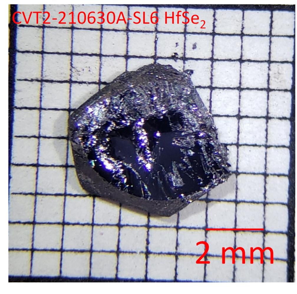 |
HfSe2 HSe2 is a semiconductor with a bulk indirect bandgap of ~1.1eV. |
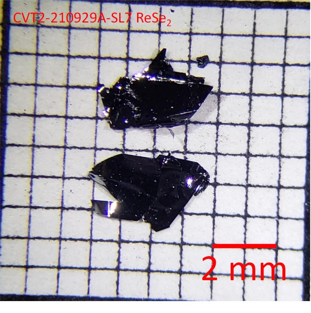 |
ReSe2 ReSe2 is a semiconductor with band gap ~1.1eV |
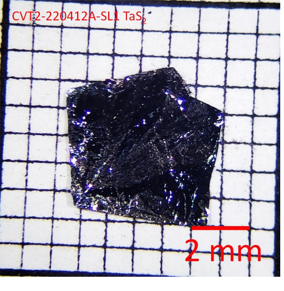 |
TaS2 TaS2 shows an incommensurate charge density waves (CDW) transition among ~80K and become superconductor at Tc~1K. |
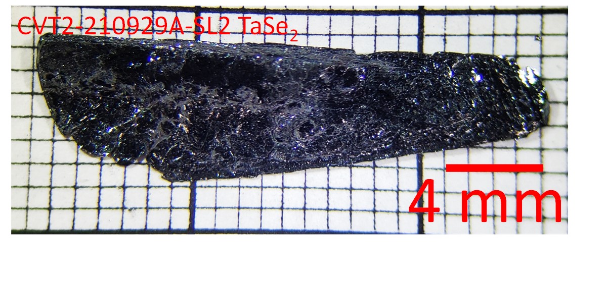 |
TaSe2 2H-TaSe2 is a metal, which shows the incommensurate Charge density waves (CDW) transition at 120K. It also become a superconductor below 0.1K. |
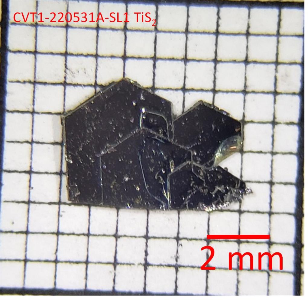 |
TiS2 TiS2 is van der Waals semimetal |
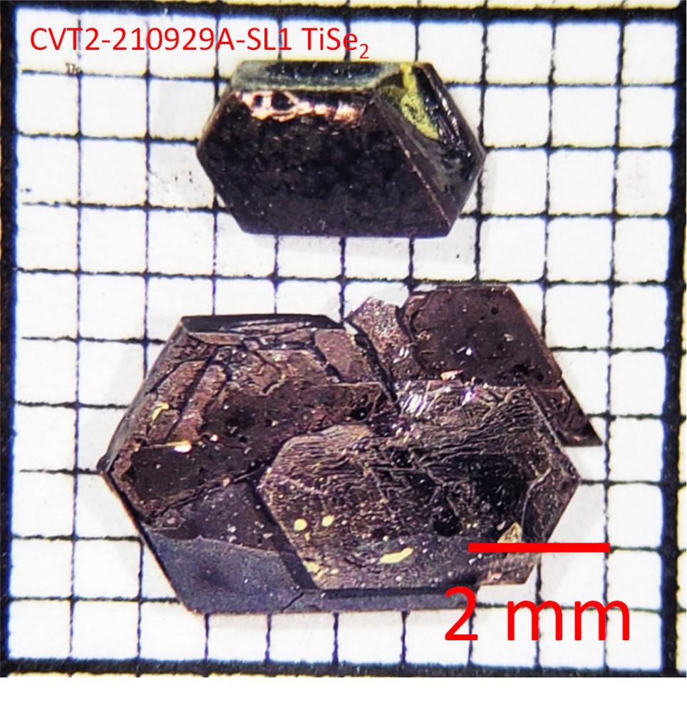 |
TiSe2 TiSe2 is a semimetal with CDW around 202 K. |
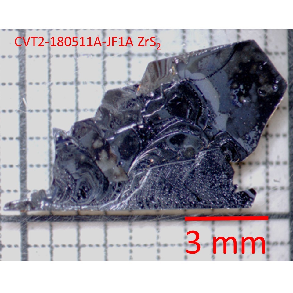 |
ZrS2 This flake was formed in an evacuated quartz ampoule by CVT synthesis method. The temperature of the source was approximately 900 °C and the crystals formed at the ampoule end that was heated to approximately 800 °C. The formation of ZrS2 is confirmed by hexagonal crystal features and Raman spectrum that matches literature reports for the material. |
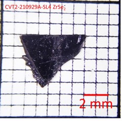 |
ZrSe2 This flake was formed in an evacuated quartz ampoule by CVT synthesis method. The temperature of the source was approximately 900 °C and the crystals formed at the ampoule end that was heated to approximately 800 °C for 200 hours. The formation of ZrSe2 is confirmed by hexagonal crystal features and Raman spectrum that matches literature reports for the material. |
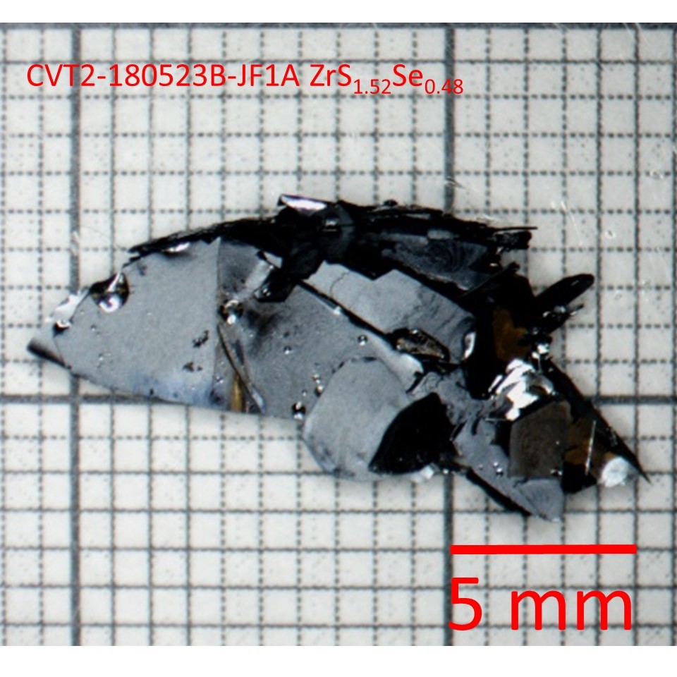 |
Zr(Se1-xSx)2 This flake was formed in an evacuated quartz ampoule by CVT synthesis method. The temperature of the source was approximately 900 °C and the crystals formed at the ampoule end that was heated to approximately 800 °C for 200 hours. The loaded source weight ratios of Zr, Se and S powder was 1:0.5:1.5 respectively. The flake is layered and a freshly cleaved surface was used for EDS composition analysis. It was found through normalized atomic % content the crystal contains an S:Se ratio of 1.52:0.48 which is very close to the source loading stoichiometry. |
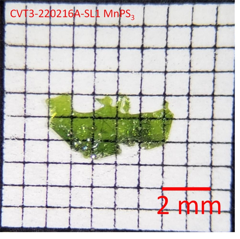 |
MnPS3 MnPS3 is a van der Waals, antiferromagnetic insulator material with Tc ~ 78 K. |
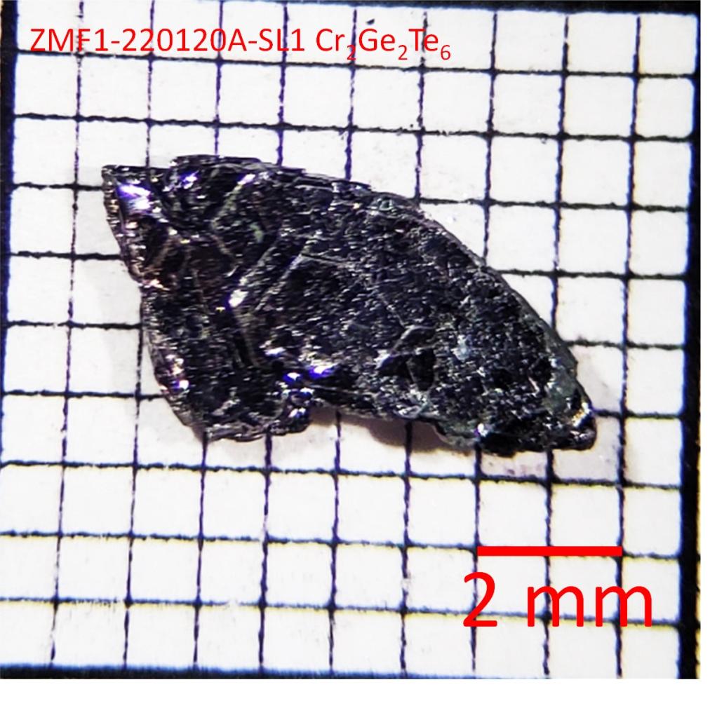 |
Cr2Ge2Te6 Cr2Ge2Te6 is a ferromagnetic insulator with a Curie temperature Tc of 61 K and is an insulator below T <100 K. |
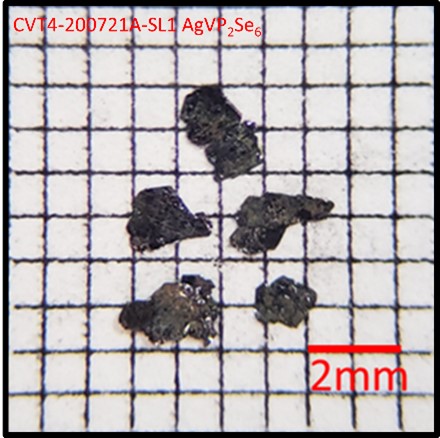 |
AgVP2Se6 AgVP2Se6 is a quaternary layered ferromagnetic semiconductor (Tc ~ 18.5K) with chiral structure. The Se-Se are bonded via weak van der Waals, allowing layers to be easily exfoliated. This metal thiophosphate material has been predicted to host the quantum anomalous Hall effect and allow for spontaneous valley splitting and valley pseudospin field effect transistor in its 2D limit. |
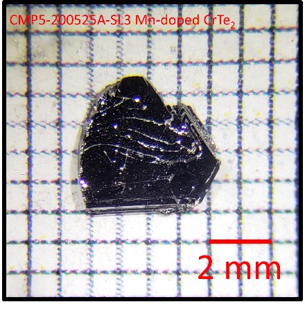 |
CrTe2 CrTe2 is a metastable layered magnetic compound with Tc at 310K. Due to the weak van der Waals bonding, the layers can be easily exfoliated. It thus offer new opportunities to study spintronic devices at room temperature. |
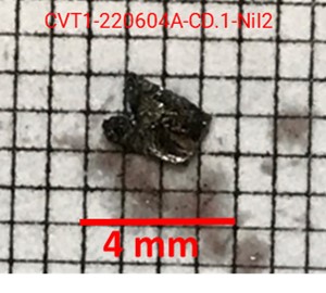 |
NiI2 A spin induced multiferroic materials (Tc = 60 K). Recently, ferroelectricity was discovered in a monolayer limit. Thus, potential candidate for future spin transport study with electrical manipulation. It can be easily exfoliate due to the van der Walls structure. |
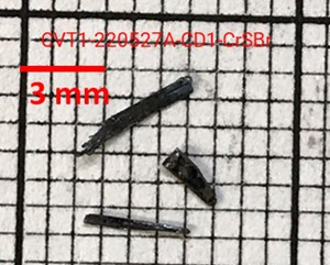 |
CrSBr Recently discovered van der Waals magnetic semiconductor. Easy plane antiferromagnetic transition TN = 142 K). Can be easily exfoliate and study the spin tunnel junction in the monolayer limit. |
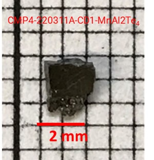 |
MnAl2Te4 Polar bulk magnetic semiconductor. Observed magnetodielectric response. A potential candidate for further exploration electronic structure and magnetotransport properties. |
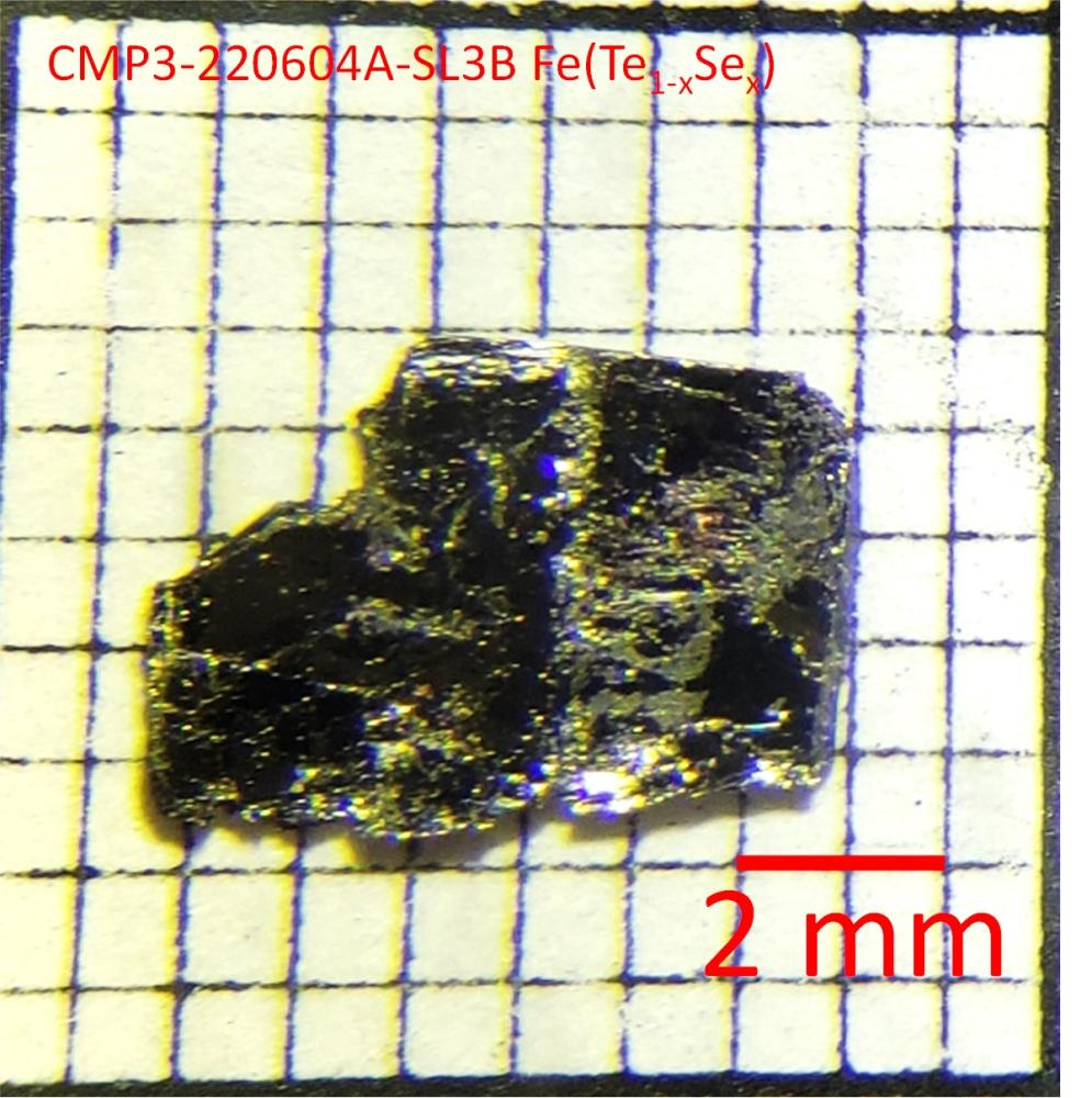 |
FeSe0.45Te0.55 FeSe0.45Te0.55 is an iron based superconductors with Tc~14K |
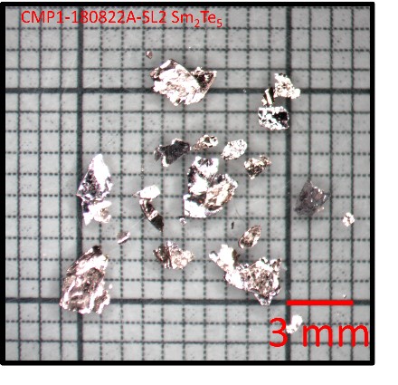 |
Sm2Te5 Sm2Te5 is a rare-earth polytelluride that has two separate charge density wave distortions of its square nets of tellurium. Due to the weak van der Waals bonding, the layers can be easily exfoliated. |
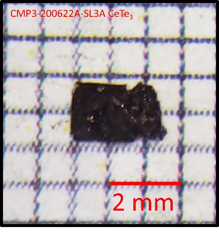 |
CeTe3 CeTe3 is one of the quasi-two-dimensional compounds with two square Te-sheets that are stacked along the b-axis. Due to its quasi 2D nature of the Te-sheet, the charge density wave is formed at room temperature.
|
|
|
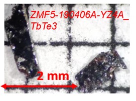
TbTe3 TbTe3 is a metal and shows CDW transition at 335K. It also exhibits a long range incommensurate magnetic order emerges at 5.78K |
|
|
NdTe3 NdTe3 is an isostructural compound to the TbTe3. It shows an AFM magnetic transition at 3K. |
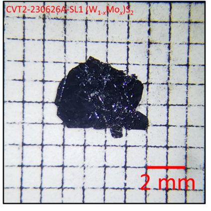 |
(W1-xMox)S2 |
|
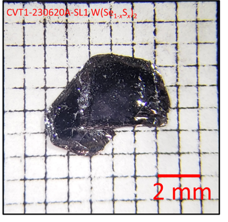 |
W(Se1-xSx)2 |
|
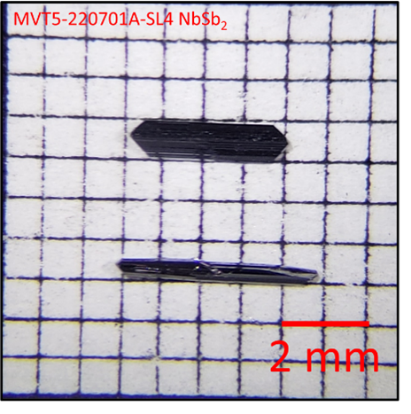 |
NbSb2 NbSb2 is a semimetal, paramagnetic ground state and non-saturation parabolic-like magnetoresistance |
|
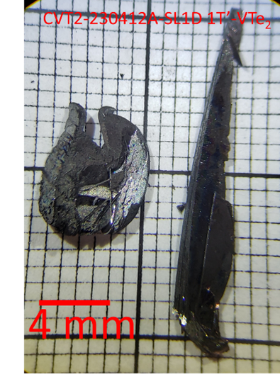 |
1T-VTe2 VTe2 is a layered transition metal dichalcogenide that shows exceptional magnetic characteristics at the 2D limit and charge density waves (CDW) property. Room temperature ferromagnetism and two possible CDW transitions have been reported in a few-layer 1T-VTe2 at 135 and 240 K |
|
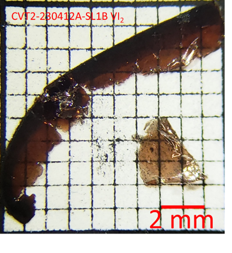 |
VI2 VI2 is a layered single crystal. It is highly sensitive to air
|
|
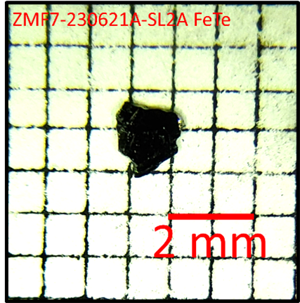 |
FeTe FeTe is a semimetal van der Waal material. This system is also an antiferromagnetic system with TN~70 K. |
|
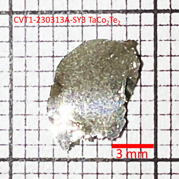 |
TaCo2Te2 TaCo2Te2 is an air-stable van der Waals material showing metallic electronic transport property as well as containing a magnetic ion. |
|
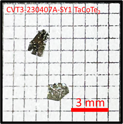 |
TaCoTe2 TaCoTe2 is a Dirac material having a van-der-Walls-type structure. Monolayer TaCoTe2 is predicted to order antiferromagnetically at around room temperature. |
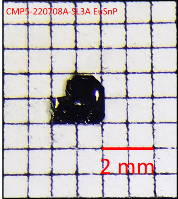 |
EuSnP EuSnP is a layered antiferromagnetic conductor with TN = 21K. |
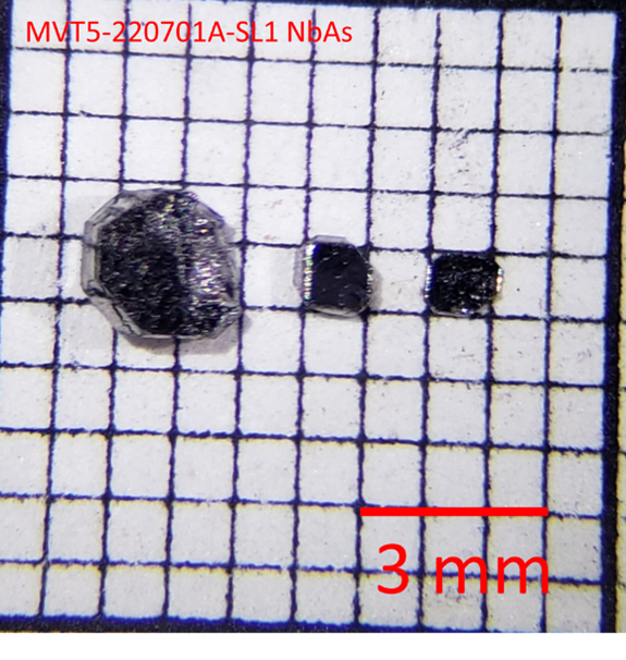 |
NbAs NbAs is experimentally verified as Weyl semimetals that contain several pairs of Weyl points. |
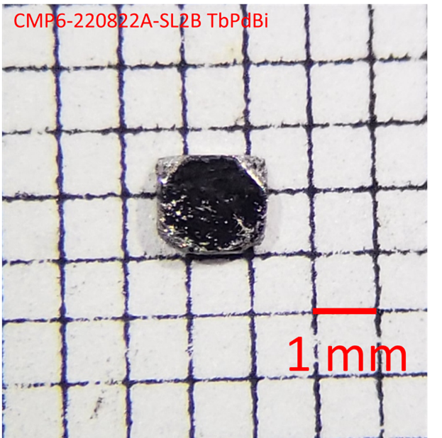 |
TbPdBi TbPdBi is an antiferromagnetic half-Heusler compound with TN = 5.2K. It possesses a surprisingly large anomalous Hall effect that originates from a half-topological semimetal state. |
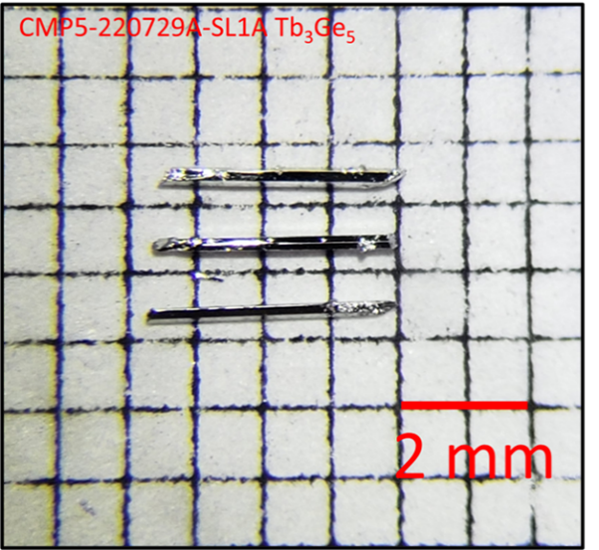 |
Tb3Ge5 Tb3Ge5 is an antifferomagnetic, non-centrosymmetry 3D crystal with TN = 17K. |
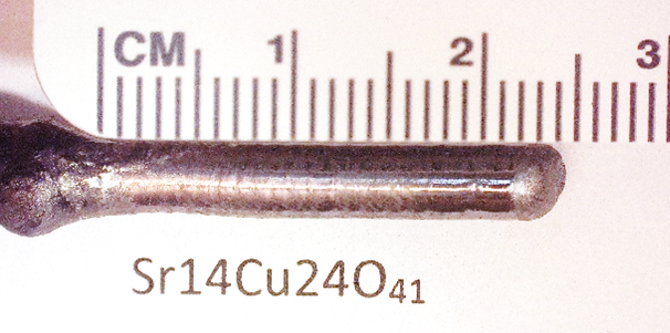 |
Sr14Cu24O41 Sr14Cu24O41 is a layered material consisting of two different types of copper oxide sheets; a CuO2 ‘chain’ layer and a Cu2O3 ‘ladder’ layer. It exhibits a charge density wave , a giant dielectric constant, and a nonlinear current–voltage curve. |
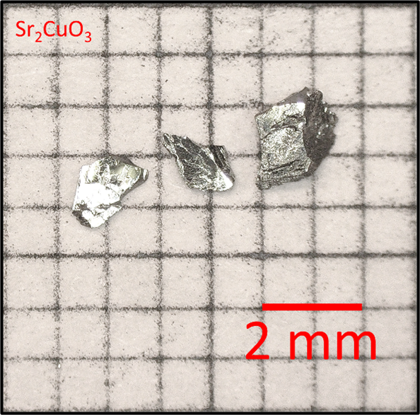 |
Sr2CuO3 Sr2CuO3 is a quasi-one-dimensional Mott insulator. Sr 2CuO3 is also found to be the best realization of the quasi-1D spin-1/2 antiferromagnetic Heisenberg model. |