
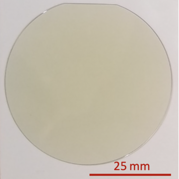
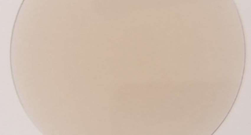
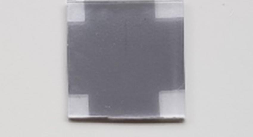
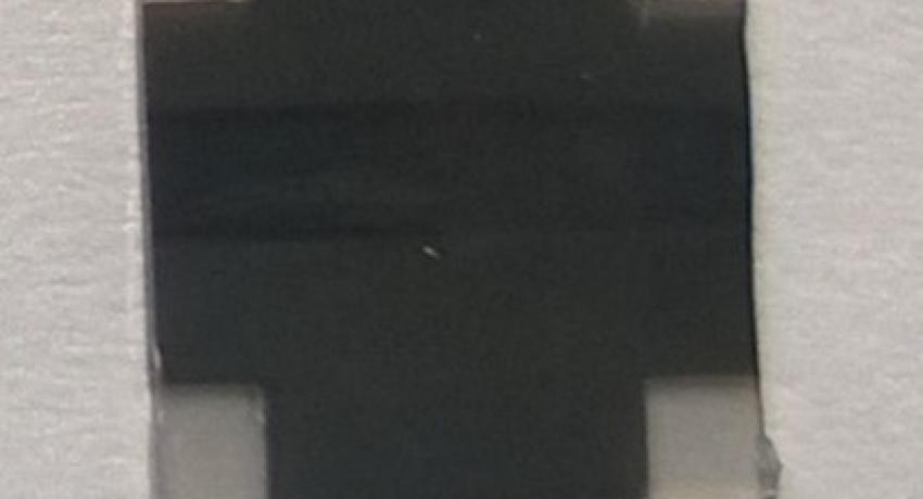
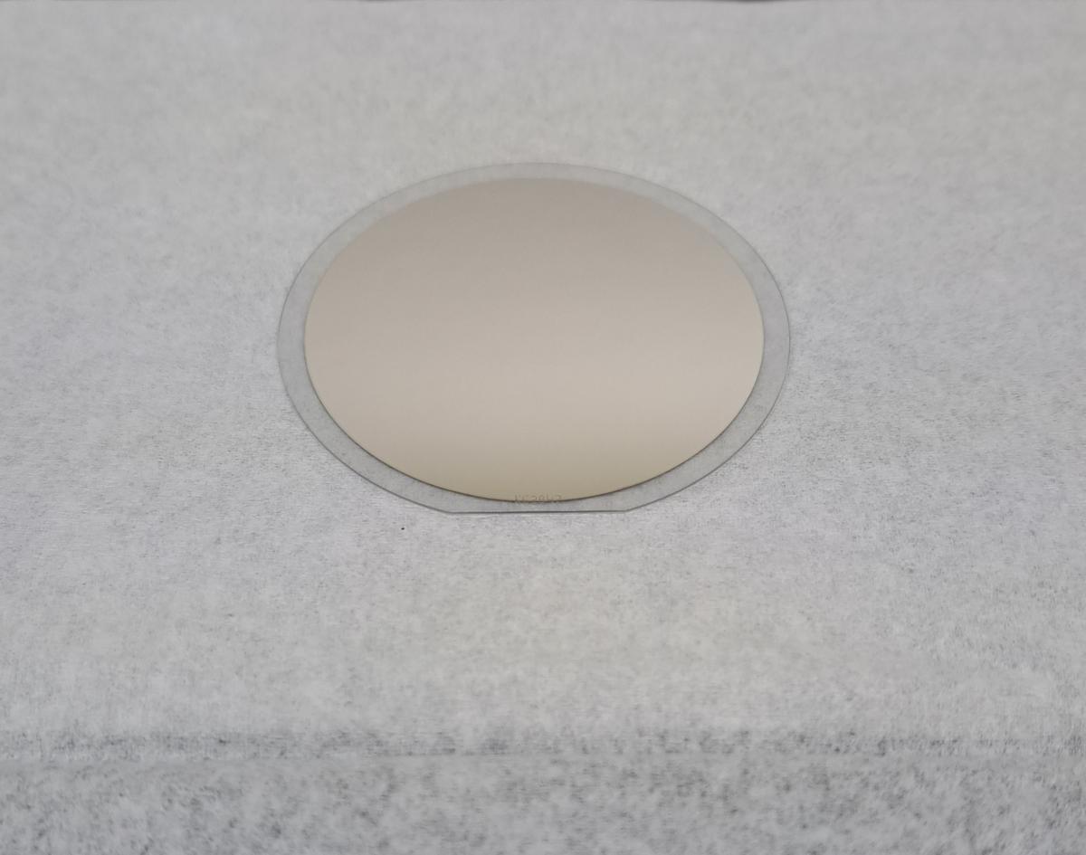
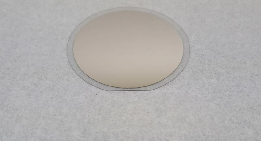
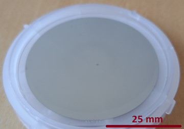
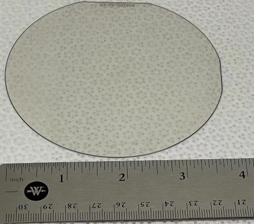
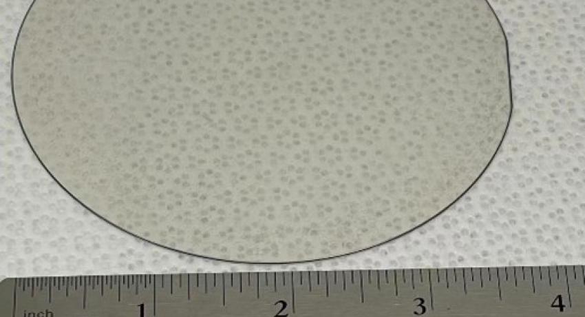
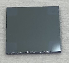
2H-WS2 in monolayer form is a semiconductor with a room temperature optical gap of ~2 eV. This sample is a continuous epitaxial film of WS2 grown by MOCVD on a 2” diameter (0001) sapphire that is monolayer with 5-15% bilayer domain coverage and inversion domain fraction ranging from 5-35% within the monolayer. See example certification sheet for more information.
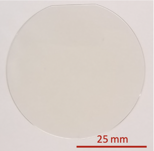
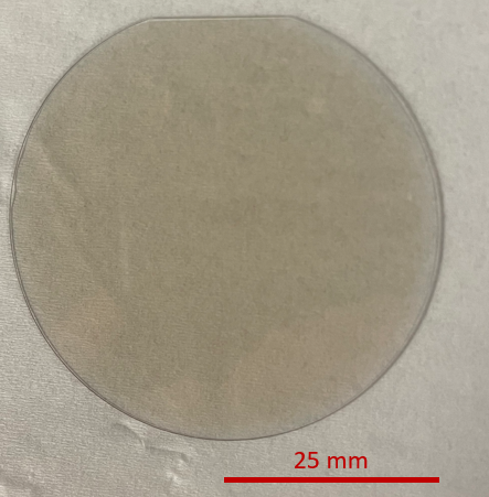
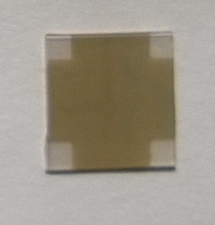
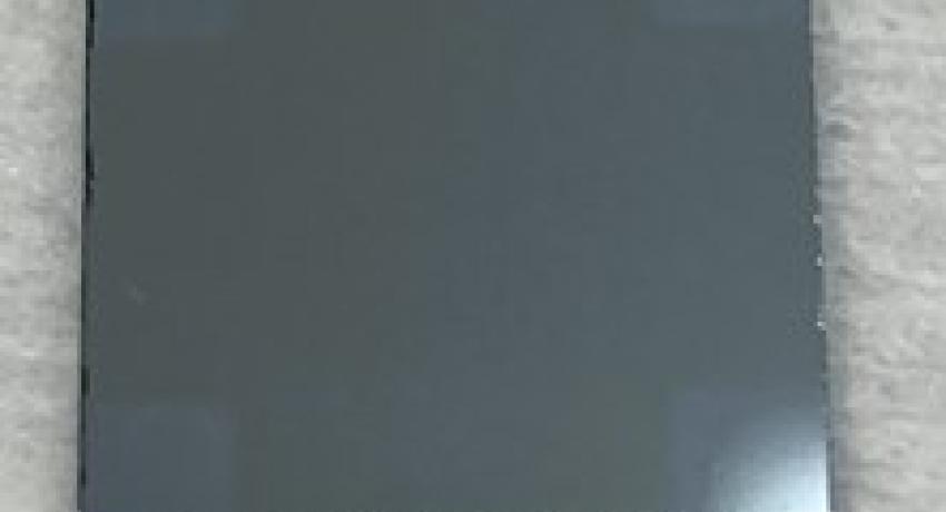
2H-MoS2 in monlayer form is a semiconductor with a room temperature optical gap of ~1.85 eV. This sample is a continuous epitaxial film of MoS2 grown by MOCVD on 2” diameter (0001) sapphire that is monolayer with 5-15% bilayer domain coverage. Inversion domain fraction has not yet been determined.
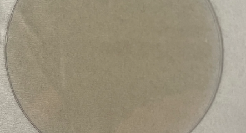
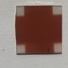
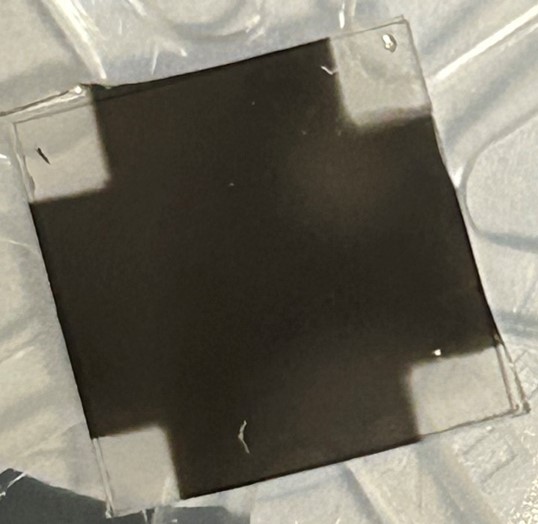
2H-WSe2 in monolayer form is a semiconductor with a room temperature optical gap of ~1.65 eV. This sample is a continuous epitaxial film of WSe2 grown by MOCVD on 2” diameter (0001) sapphire that is monolayer with 20% bilayer domain coverage. Inversion domain fraction has not yet been determined.
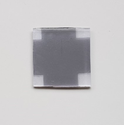
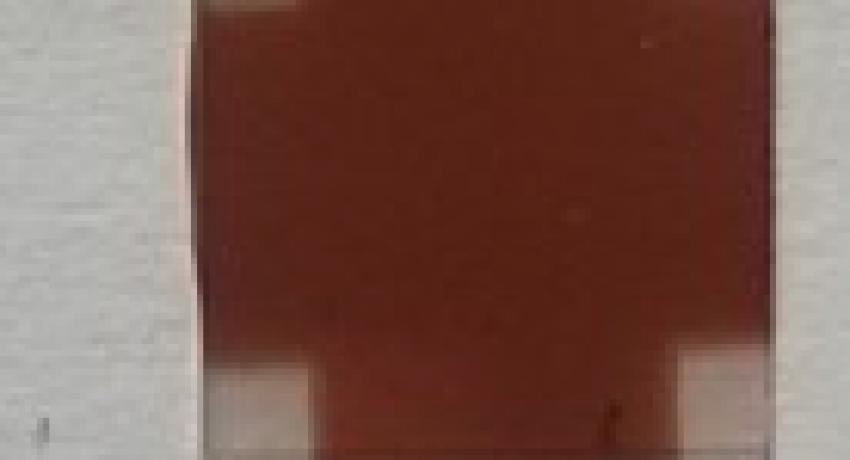
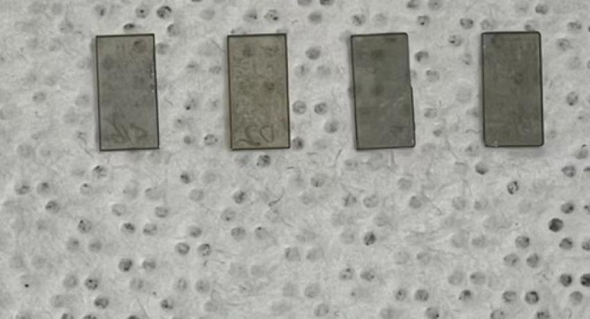
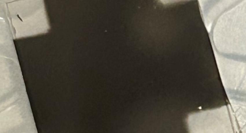
Our 2H-WSe2 multi-layer films are a semiconductor with a uniform distribution of Raman spectra breathing mode at 310 cm-1 at room temperature. This sample is a continuous epitaxial film of WSe2 grown by MOCVD on 1 cm × 1 cm (0001) sapphire that is >95% bilayer with 30-40% trilayer domain coverage. Inversion domain fraction has not yet been determined.
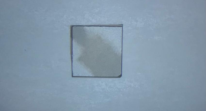
Bulk PtSe2 is a layered semimetal but in the monolayer form it is semiconducting with an optical gap of ~1.2 eV. PtSe2 ranges among the highest room-temperature electron mobility two-dimensional materials and is air-stable. This sample is a continuous epitaxial film of PtSe2 grown on (10x10) mm square (0001) sapphire. The PtSe2 layer is single crystal with not yet determined inversion domain fraction, the thickness can be adjusted from one single layer to few-layers.
In2Se3 is a trivial bandgap semiconductor with a band gap of about 1.3 eV and reported room-temperature ferroelectricity depending on the phase. Among the many In2Se3 phases phase pure single crystal thin films of alpha- and gamma-In2Se3 are available on (10x10) mm square or 3” diameter wafers of (0001) sapphire or (111) Si with thicknesses ranging from one to few quintuple layers.
Bulk InSe is a direct semiconductor with a band gap of 1.4 eV. In the fewlayer limit the band gap increases and a crossover to an indirect gap is observed that forms a weakly dispersive “Mexican hat” valence band. Even in the monolayer limit, InSe is still optically active and air stable. The low exciton and electron effective masses make InSe a high-mobility semiconductor with longer electron and hole spin relaxation times than GaAs and excellent photoresponsivity. InSe possesses many phases that are composed of individual quadruple atomic In-Se-Se-In layers. The stacking order of the quadruple sheets determines the InSe phase. InSe is available in a variety of stacking orders and adjustable thicknesses.
Thin films of the topological insulator Bi2Se3 with a band gap of about 0.3 eV are available with single to few-layer thickness on 3” diameter or (10x10) mm (0001) sapphire wafers or (10x10) mm square (111)A InP. Direct growth of Bi2Se3 on sapphire or InP yields n-type material with carrier concentrations in the low 1020 cm-3 range and room-temperature mobilities below 500 cm2/Vs. Improved mobilities around 1000 cm2/Vs at room temperature and one order of magnitude lower carrier concentrations are obtained for Bi2Se3 films grown on a buffer layer of In2Se3 and (Bi0.5In0.5)2Se3.
The monochalcogenide alpha SnSe is a layered semiconductor with a band gap around 1.2 eV that exhibits remarkable in-plane ferroelectric distortion, which results in record-high thermoelectric performance, piezo- and ferroelectricity, and phase-change behavior. Phase pure alpha-SnSe is available in adjustable thickness on (100) MgO with twinned inversion domain fractions of about 50/50 and on (11 20) sapphire with suppressed high-angle inversion domain formation.
Bulk FeSe is a semimetallic superconductor with a Curie temperature of 9 K but thin films on SrTiO3 in the mono- to few-layer limit possess much higher Curie temperatures. Thin FeSe films of various thickness are available with FeTe and a-Te or a-Se capping with reliable Curie temperatures at or above 15 K and superconductivity onset temperatures around 50 K in ex-situ physical property measurements.
(Cr and V doping available)
(BixSb1-x)2Te3 is topological insulator with a band gap of ~0.15 eV, depending on composition. The carrier density of our MBE grown thin films can be tuned with the Bi to Sb ratio so that the chemical potential can be placed very near the Dirac point. With Cr or V doping this allows samples that exhibit the quantum anomalous Hall effect (QAHE). SrTiO3 substrates can be used to back gate the samples. Se or Te capping is also available.
ZrTe2 is a 2D van der Waals layered material has a 1T crystal structure. It is a Dirac semimetal with a topological bandstructure. On sapphire, films with thicknesses of 3 layers and above can be grown on wafers up to 2” in diameter, while single layer films on epi-graphene are possible on substrates up to 10 mm x 5 mm. Films are very sensitive to air exposure and need to be capped with Te.
CrTe2 is a layered ferromagnet material with a Curie temperature Tc above room temperature in the bulk form, while its monolayer still maintains the ferromagnetic order, but with a Tc lower than room temperature, making it a candidate material for two-dimensional ferromagnets. Samples up to 10 x 10 mm can be grown and are typically capped with Te.
FeSe is a layered material known for its enhanced onset superconducting critical temperature when grown on SrTiO3 substrates (40 K) compared to its bulk crystal counterpart (9 K). By substituting tellurium for selenium in controlled amounts, the FeTeSe ternary system becomes a candidate platform for the realization of topological superconductivity. Films up to 10 x 10 mm can be grown. These samples are very sensitive to air and can be capped with either crystalline FeTe and amorphous tellurium, or amorphous selenium which can later be removed.
Epitaxial graphene was formed on 6H-SiC (0001) in a graphite crucible via Si sublimation from the Si side of the substrate. By tuning the experimental conditions, EG samples with different thicknesses ranging from a buffer layer to 2-3 layers and up to 4” wafer scale size can be synthesized in a highly controlled fashion.
Two Dimensional Ga, Ag, In and Ga/In alloy are formed between bilayer graphene and SiC substrates via confinement heteroepitaxy (CHet). The thickness of 2D metals varies from 1~3 layers. The overlying graphene layers not only help confine 2D metal, but also prevent ultra-thin metal film from oxidation. 2D Ga is a superconductor and its Tc is ~3.95K. Monolayer Ag is Ag confined between bilayer graphene and SiC is a large gap (> 1 eV) 2D semiconductor. The Ga percentage in 2D Ga/In alloy can be tuned from 0~100% via CHet process.
Bulk 2H-GaSe is a direct p-type semiconductor with a bandgap of 2.1 eV. In the few-layer limit (~3 monolayers), the bandgap increases and a crossover to an indirect gap of 3.3 eV is observed. GaSe has four polytypes due to the different stacking sequences of the individual tetra-atomic Ga-Se-Se-Ga layers. This sample is a continuous epitaxial film of 30 monolayers (001)-oriented 2H-GaSe grown by MBE on a 1 cm×1 cm GaAs (111)B substrate. In-plane inversion domains are found to some degree in the film.
MnBi2Se4 is an intrinsic magnetic topological insulator with a Curie temperature around 10 K. Above the Curie temperature it has a Dirac-like surface state. Below the Curie temperature, in layered form, it is antiferromagnetic. This sample is 20 septuple layers of MnBi2Se4 grown by MBE. The thickness can be adjusted from one single layer to few-layers.