
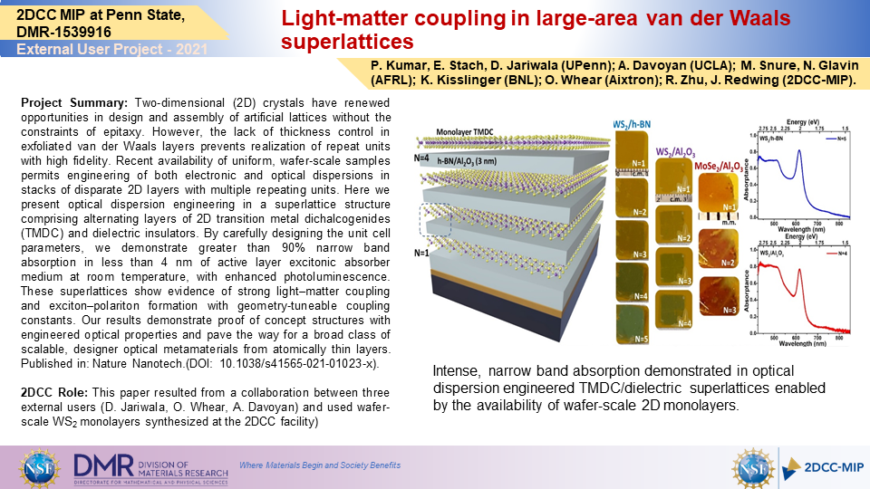
Project Summary: Two-dimensional (2D) crystals have renewed opportunities in design and assembly of artificial lattices without the constraints of epitaxy. However, the lack of thickness control in exfoliated van der Waals layers prevents realization of repeat units with high fidelity. Recent availability of uniform, wafer-scale samples permits engineering of both electronic and optical dispersions in stacks of disparate 2D layers with multiple repeating units. Here we present optical dispersion engineering in a superlattice structure comprising alternating layers of 2D transition metal dichalcogenides (TMDC) and dielectric insulators. By carefully designing the unit cell parameters, we demonstrate greater than 90% narrow band absorption in less than 4 nm of active layer excitonic absorber medium at room temperature, with enhanced photoluminescence. These superlattices show evidence of strong light–matter coupling and exciton–polariton formation with geometry-tuneable coupling constants. Our results demonstrate proof of concept structures with engineered optical properties and pave the way for a broad class of scalable, designer optical metamaterials from atomically thin layers. Published in: Nature Nanotech.(DOI: 10.1038/s41565-021-01023-x).
2DCC Role: This paper resulted from a collaboration between three external users (D. Jariwala, O. Whear, A. Davoyan) and used wafer-scale WS2 monolayers synthesized at the 2DCC facility)
What Has Been Achieved: Design, fabrication and characterization of large area superlattices that combine alternating layers of monolayer transition metal dichalcogenides and ultra-thin dielectrics (hBN and Al2O3). Spacing the TMDC monolayers between dielectrics enables them to retain a direct bandgap and consequently yields high absorption (over 90%) with only 4 nm of active excitonic material and exciton-polariton formation.
Importance of the Achievement: The results demonstrate proof of concept structures with engineered optical properties that pave the way for a broader class of scalable, engineered optical metamaterials from 2D layers.
Unique Feature(s) of the MIP that Enabled this Achievement: The fabrication of the superlattice structures was enabled by the availability of high optical quality wafer-scale WS2 monolayers synthesized in the 2DCC facility. The project was led by an external user, Deep Jariwala, at UPenn and included participation of two other 2DCC external users including Oliver Whear at Aixtron who provided large area hBN films and Artur Davoyan at UCLA who assisted with optical design.
(If Applicable) Publication:
P. Kumar, et al., “Light-matter coupling in large-area van der Waals superlattices,” Nature Nanotech. https://doi.org/10.1038/s41565-021-01023-x
Support for the work at UPenn (D.J) was provided by the US Army Research Office under contract number W911NF-19-1-0109 and Air Force Office of Scientific Research (AFOSR) grant no. FA9550-21-1-0035. E.S. acknowledges support from the National Science Foundation (NSF) (grant no. DMR-1905853) and support from University of Pennsylvania Materials Research Science and Engineering Center (MRSEC) (grant no. DMR-1720530) in addition to usage of MRSEC supported facilities. The sample fabrication, assembly and characterization were carried out at the Singh Center for Nanotechnology at the University of Pennsylvania, which is supported by the NSF National Nanotechnology Coordinated Infrastructure Program grant no. NNCI-1542153. F.B. is supported by the Vagelos Integrated Program in Energy Research. H.Z. was supported by Vagelos Institute of Energy Science and Technology graduate fellowship. S.B.A acknowledges support from Swiss National Science Foundation Early Postdoc Mobility Program (P2ELP2_187977). A.R.D. acknowledges support of NG Next, UCLA Council on Research Faculty Research grant and the Hellman Foundation. The TMDC monolayer samples were provided by the 2D Crystal Consortium-Materials Innovation Platform (2DCC-MIP) facility at the Pennsylvania State University, which is funded by the NSF under cooperative agreement no. DMR-1539916. M.S. and N.R.G. acknowledge support from the Air Force Office of Scientific Research under award no. FA9550-19RYCOR050. This research used resources of the Center for Functional Nanomaterials, which is a US Department of Energy Office of Science User Facility, at Brookhaven National Laboratory under contract no. DE-SC0012704.