
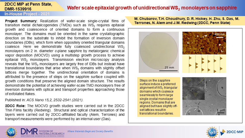
Project Summary: Realization of wafer-scale single-crystal films of transition metal dichalcogenides (TMDs) such as WS2 requires epitaxial growth and coalescence of oriented domains to form a continuous monolayer. The domains must be oriented in the same crystallographic direction on the substrate to inhibit the formation of inversion domain boundaries (IDBs), which form when oppositely oriented triangular domains coalesce. Here we demonstrate fully coalesced unidirectional WS2 monolayers on 2 in. diameter c-plane sapphire by metalorganic chemical vapor deposition (MOCVD) using a multistep growth process to achieve epitaxial WS2 monolayers. Transmission electron microscopy analysis reveals that the WS2 monolayers are largely free of IDBs but instead have translational boundaries that arise when WS2 domains with slightly offset lattices merge together. The unidirectional orientation of domains is attributed to the presence of steps on the sapphire surface coupled with growth conditions that preserve the aligned domain structure. The results demonstrate the potential of achieving wafer-scale TMD monolayers free of inversion domains with optical and transport properties approaching those of exfoliated flakes.
Published in: ACS Nano 15,2, 2532-2541 (2021).
2DCC Role: The MOCVD growth studies were carried out in the 2DCC Thin Films facility (Redwing). Structural and optical characterization of the layers were carried out by 2DCC-affiliated faculty (Alem, Terrones) and transport measurements were performed by an internal user (Das).
What Has Been Achieved: Epitaxial WS2 monolayers on 2” diameter sapphire that exhibit a unidirectional alignment of domains resulting in coalesced films that are largely free of inversion domain boundaries.
Importance of the Achievement: A persistent problem in epitaxial growth of transition metal dichalcogenides has been the formation of inversion domain boundaries (also referred to as mirror twins) which arise when oppositely oriented TMD domains coalesce. The twin boundaries exhibit a metallic character which introduces conducting channels in the semiconducting monolayer. Inversion domains also are problematic for studying spin-valley polarization which relies on a uniform crystallographic direction. This work demonstrates that steps on the sapphire surface can induce a preferred alignment of domains resulting in coalesced WS2 monolayers that are largely free of inversion domain boundaries. Instead, the dominant defects are translational boundaries that arise when TMD domains that are off-set from one another by less than a unit cell coalesce. WS2 monolayers that are 95% single crystal (<5% of monolayer contains transitional boundaries) have been obtained.
Unique Feature(s) of the MIP that Enabled this Achievement: 2DCC-MIP’s MOCVD equipment that enables uniform growth on substrates up to 2” in diameter using high purity hydride precursors. Internal collaborations with 2DCC affiliated faculty and internal users with expertise in TEM, optical characterization and transport measurements.
(If Applicable) Publication: M. Chubarov, T.H. Choudhury, D. Reifsnyder Hickey, S. Bachu, T. Zhang, A. Sebastian, A. Bansal, H. Zhu, N. Trainor, S. Das, M.Terrones, N. Alem and J.M. Redwing, “Wafer scale epitaxial growth of unidirectional WS2 monolayers on sapphire,”, ACS Nano. 2021, 15,2 2532-2541. https://doi.org/10.1021/acsnano.0c06750.
Acknowledgments: Primary financial support for this work was provided by the National Science Foundation (NSF) through the 2D Crystal Consortium–Materials Innovation Platform (2DCC-MIP) under NSF cooperative agreement DMR-1539916. D.R.H., S.B., and N.A. acknowledge additional support from an NSF CAREER grant (DMR-1654107). T.Z. and M.T. acknowledge the financial support of the Air Force Office of Scientific Research (AFOSR) through grant FA9550-18-1-0072. The work of S.D. and A.S. was partially supported by Army Research Office through Cooperative Agreement Grant W911NF1920338 and Air Force Office of Scientific Research (AFOSR) through the Young Investigator Program Grant FA9550-17-1-0018. This work utilized resources provided by the NSF-MRSEC-sponsored Materials Characterization Lab at Pennsylvania State University.