
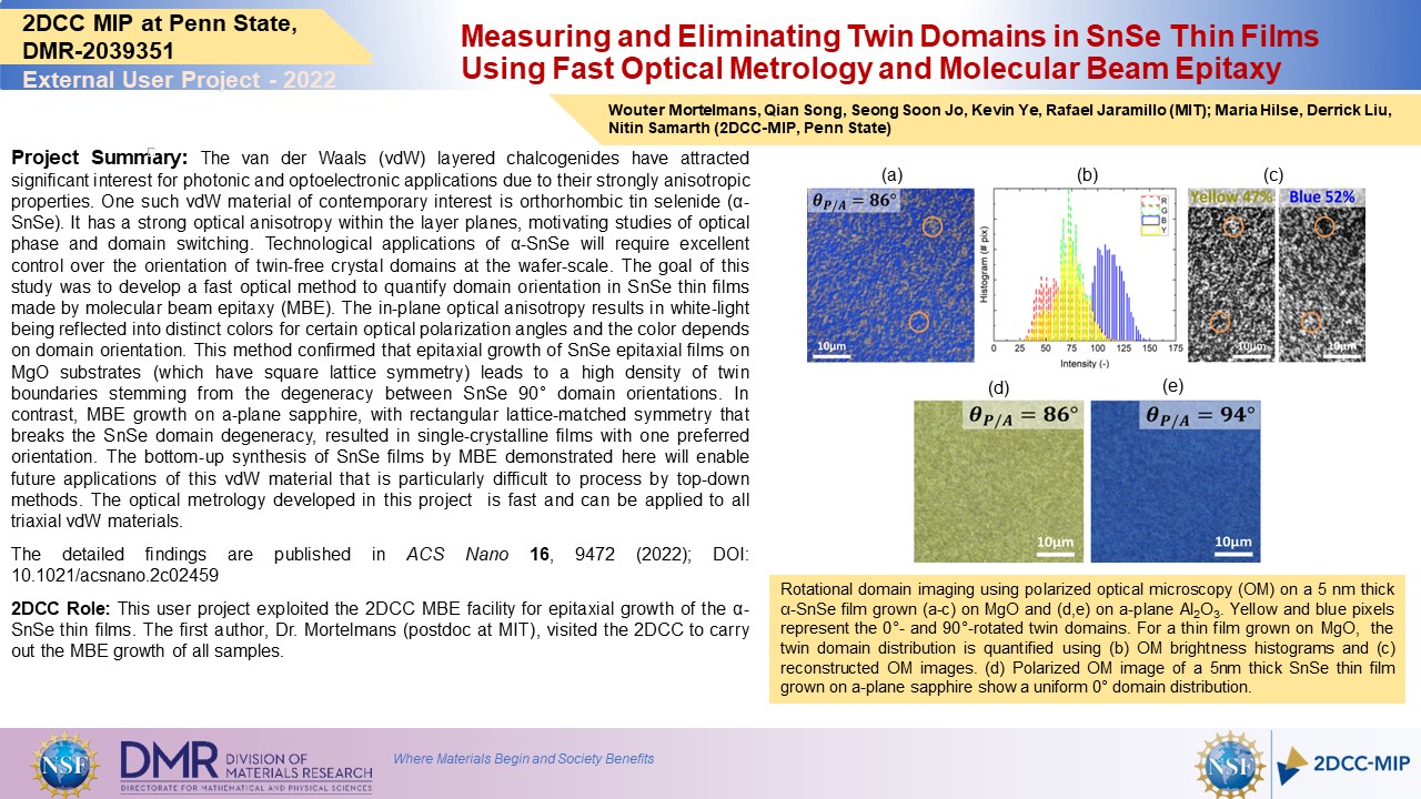
Project Summary: The van der Waals (vdW) layered chalcogenides have attracted significant interest for photonic and optoelectronic applications due to their strongly anisotropic properties. One such vdW material of contemporary interest is orthorhombic tin selenide (α-SnSe). It has a strong optical anisotropy within the layer planes, motivating studies of optical phase and domain switching. Technological applications of α-SnSe will require excellent control over the orientation of twin-free crystal domains at the wafer-scale. The goal of this study was to develop a fast optical method to quantify domain orientation in SnSe thin films made by molecular beam epitaxy (MBE). The in-plane optical anisotropy results in white-light being reflected into distinct colors for certain optical polarization angles and the color depends on domain orientation. This method confirmed that epitaxial growth of SnSe epitaxial films on MgO substrates (which have square lattice symmetry) leads to a high density of twin boundaries stemming from the degeneracy between SnSe 90° domain orientations. In contrast, MBE growth on a-plane sapphire, with rectangular lattice-matched symmetry that breaks the SnSe domain degeneracy, resulted in single-crystalline films with one preferred orientation. The bottom-up synthesis of SnSe films by MBE demonstrated here will enable future applications of this vdW material that is particularly difficult to process by top-down methods. The optical metrology developed in this project is fast and can be applied to all triaxial vdW materials.
The detailed findings are published in ACS Nano 16, 9472 (2022); DOI: 10.1021/acsnano.2c02459
2DCC Role: This user project exploited the 2DCC MBE facility for epitaxial growth of the α-SnSe thin films. The first author, Dr. Mortelmans (postdoc at MIT), visited the 2DCC to carry out the MBE growth of all samples.
What Has Been Achieved: This paper reported the development of a fast optical method to characterize the presence of twin domains in wafer scale films of a 2D van der Waals (vdW) material, alpha-SnSe. This method was exploited to characterize the formation of twin domains during MBE growth of alpha-SnSe films grown on MgO and then used to demonstrate a vast improvement in the crystalline quality of these films by using an appropriate symmetry-matched substrate (a-plane sapphire).
Importance of the Achievement: The results establish a convenient and rapid methodology for characterizing the structural quality of vdW thin films at the wafer scale. This provides quick feedback to MBE growers seeking to improve the quality of thin films.
Unique Feature(s) of the MIP that Enabled this Achievement: The achievement was enabled by significant 2DCC expertise in the MBE growth of 2D chalcogenides.
(If Applicable) Publication:
Wouter Mortelmans, Maria Hilse, Qian Song, Seong Soon Jo, Kevin Ye, Derrick Liu, Nitin Samarth, Rafael Jaramillo, ACS Nano 16, 9472 (2022); DOI: 10.1021/acsnano.2c02459
Acknowledgements: This work was supported by the Office of Naval Research (ONR) MURI through grant nos. N00014-17-1-2661 and N00014-20-1-2807. This study is based upon research conducted at The Pennsylvania State University Two-Dimensional Crystal Consortium – Materials Innovation Platform (2DCC-MIP) which is supported by NSF cooperative agreement NSF DMR-2039351.