
What Has Been Achieved:
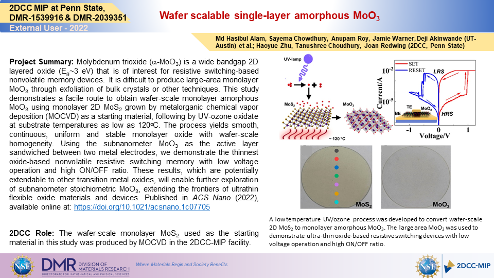
A process to produce wafer-scale single-layer amorphous MoO3 was developed by UV-ozone oxidation of a MoS2 monolayer. The ultrathin MoO3 was used an active device layer to demonstrate the thinnest oxide-based nonvolatile resistive switching device that exhibits low voltage operation and high ON/OFF ratio.
Importance of the Achievement:
It has been challenging to fabricate large area single-layer transition metal oxides using exfoliation or vapor phase deposition methods. The process is demonstrated for MoO3 but can be extended to other transition metal oxides such as WO3.
Unique Feature(s) of the MIP that Enabled this Achievement:
Uniform monolayer MoS2 films grown on 2” diameter c-plane sapphire in the MOCVD1 system were provided to the user for this study.
Publication:
M.H. Alam, S. Chowdhury, A. Roy, X. Wu, R. Ge, M.A. Rodder, J. Chen, Y. Lu, C. Stern, L. Houben, R. Chrostowski, S.R. Burlison, S.J. Yang, M.I. Serna, A. Dodabalapur, F. Mangolini, D. Naveh, J.C. Lee, S.K. Banerjee, J.H. Warner and D. Akinwande, ACS Nano (2022), available online at: https://doi.org/10.1021/acsnano.1c07705
D.A. acknowledges the PECASE award from the Army Research Office (ARO) grant #W911NF-16-1-0277 and the National Science Foundation (NSF) MRSEC Center (DMR-172059). S.K.B. acknowledges support from ARO grant #W911NF-17-1-0312 (MURI) and the NSF NASCENT ERC. The development of the XPS peak fitting model was supported by the Laboratory Directed Research and Development program at Sandia National Laboratories, a multimission laboratory managed and operated by National Technology and Engineering Solutions of Sandia LLC, a wholly owned subsidiary of Honeywell International Inc. for the U.S. Department of Energy’s National Nuclear Security Administration under contract DE-NA0003525. The work was partly done at the Texas Nanofabrication Facility supported by NSF grant #NNCI-1542159. The authors would like to thank Haoyue Zhu, Tanushree H. Choudhury, and Joan M. Redwing of 2D Crystal Consortium-Materials Innovation Platform (2DCC-MIP) which is funded by the NSF cooperative agreements DMR-1539916 and DMR-2039351 at Penn State University, for providing the wafer-scale MoS2 samples. In addition, the authors would like to thank Kun Li of Microelectronics Research Center for taking the optical micrograph of the sapphire wafers. The authors also thank Jo Wozniak of the Texas Advanced Computing Center (TACC) for helping with the three-dimensional renderings.
Credits/Names: Md Hasibul Alam, Sayema Chowdhury, Anupam Roy, Jamie Warner, Deji Akinwande (UT-Austin) et al.; Haoyue Zhu, Tanushree Choudhury, Joan Redwing (2DCC, Penn State)
Download PDF Version: 1539916-2039351_2DCCMIP_2022_Wafer Scalable Single-layer Amorphous MoO3.pdf
Year of Research Highlight: 2021
Select a Highlight Type: User Highlight