The dates for the 2025 undergraduate summer research program are May 27 - July 31, 2025.
Please apply now. Applications will be reviewed as they are received and offers will be made starting in late January 2025.
The stipend is $6,600 for the summer.
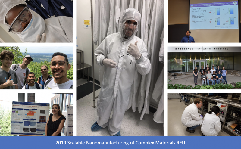 Co-hosted by researchers at the Penn State Nanofabrication and the 2D Crystal Consortium – Materials Innovation Platform user facilities, the Nanomanufacturing of Emerging 2D Materials and Devices summer undergraduate research program provides undergraduate students with an opportunity to experience research within a small team environment reflective of the organizational structure typical of the semiconductor industry. Undergraduate students work as part of small interdisciplinary research team that includes other fellow undergraduate summer researchers, their faculty advisors and graduate student mentors, all of whom working together towards a novel device or process development goal. Each undergraduate has an individual responsibility on the team and questions to investigate that tie directly into the overall team objectives. The undergraduate students also receive training in responsible conduct of research, data management, and laboratory safety; and they take part in professional development opportunities, interact with engineers in the semiconductor industry, and participate in social activities.
Semiconductor technology in the United States is entering a new era propelled by emerging demands in 5G, artificial intelligence (AI) and Internet-of-Things (IoT) and new opportunities in domestic manufacturing enabled by the CHIPs Act. It is estimated that the US will require at least 50,000 new semiconductor scientists and engineers over the next 5 years to meet the goals of the CHIPs act alone.1 The semiconductor industry is rapidly approaching the end of Moore’s law in terms of device scaling using Si-based transistors. Thus, moving forward, it is essential to train the semiconductor R&D workforce not only in traditional sectors (e.g., silicon processing) but also in emerging and converging areas (e.g., More-than-Moore electronics). Critical to this vision is the ability to integrate diverse materials, which will necessitate new manufacturing paradigms for materials that fall outside of the traditional cleanroom materials subset. Our summer undergraduate research program focusses specifically on two-dimensional (2D) semiconductors, a class of layered van der Waals crystals that offer unique performance benefits in a range of emerging device technologies and the potential to be readily integrated with silicon CMOS and other materials to realize new functionalities. 2D semiconductors of specific interest include the transition metal dichalcogenides (TMDs) such as MoS2 and WSe2, which become direct gap at the monolayer limit and exhibit superior transport properties compared to silicon in aggressively scaled devices due to their self-passivated nature.2 2D TMDs with their high surface to volume ratio and accessibility to surface functionalization are also well-suited for chemical and biological sensors that can be exploited in More-than-Moore electronics.3 Another application space for 2D TMDs is in brain-inspired neuromorphic computing to realize energy efficient hardware for AI and edge computing for IoT.4 In addition to the TMDs, topological 2D materials such as Bi2Se3 and Bi2Te3 and related alloys, which are narrow gap semiconductors, can be used to manipulate magnetic ordering in ferromagnets for applications in non-volatile memory and logic5 and are also under intense investigation for quantum devices.6
If you would like to join us as part of the cohort of undergraduate students this summer, please fill out our application form. This program is open to all U.S. citizens or permanent residents.
Apply Now
References
1. https://www.electronicdesign.com/technologies/analog/article/21247302/e… (last accessed August 29, 2022)
2. D. Akinwande, C. Huyghebaert, C.H. Wang, M.I. Serna, S. Goossens, L.J. Li, H.S. P. Wong, F.H.L. Koppens, “Graphene and two-dimensional materials for silicon technology,” Nature 573, 507–518 (2019) DOI: 10.1038/s41586-019-1573-9
3. Joshua J. Fox, Xiaotian Zhang, Zakaria Y. Al Balushi, Mikhail Chubarov, Azimkhan Ko-zhakhmetov, and Joan M. Redwing, “Van der Waals epitaxy and composition control of lay-ered SnSxSe2-x alloy thin films,” Journal of Materials Research 35, 1386–1396 (2020) DOI: 10.1557/jmr.2020.19M.C. Lemme, D. Akinwande, C. Huyghebaert, C. Stampfer, “2D materials for future heteroge-neous electronics,” Nature Comm. 13 1392-1–1392-4 (2022) DOI: 10.1038/s41467-022-29001-4
4. A.R. Mellnick, J.S. Lee, A. Richardella, J.L. Grab, P.J. Mintum, M.H. Fischer, A. Vaezi, A. Manchon, E.A. Kim, N. Samarth, D.C. Ralph, “Spin-transfer torque generated by a topological insulator,” Nature 511 449–451 (2014) DOI: 10.1038/nature13534
5. O. Breunig, Y. Ando, “Opportunities in topological insulator devices,” Nature Rev. Physics 4 184–193 (2022) DOI: 10.1038/s42254-021-00402-6
6. A. P. Jacob, R. Xie, M. G. Sung, L. Liebmann, R. T. Lee, and B. Taylor, "Scaling challenges for advanced CMOS devices," International Journal of High Speed Electronics and Systems, 26, 1740001 (2017) DOI: 10.1142/S0129156417400018