

Scanning Electron Microscopy (SEM) uses a focused electron beam to scan a solid sample from the millimeter to the nanometer range. Secondary electrons are generated in the sample and collected to create a map of the secondary emissions. Since the intensity of secondary emission is dependent on local morphology, the area map is a magnified image of the sample. Spatial resolution smaller than 1 nanometer is possible for our FE-SEM instruments. Backscattered electrons (BSE) and characteristic X-rays are also generated by the scanning beam and many instruments employ these signals for compositional analysis of the sample.
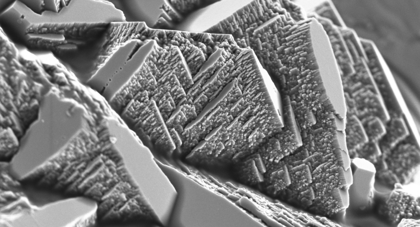
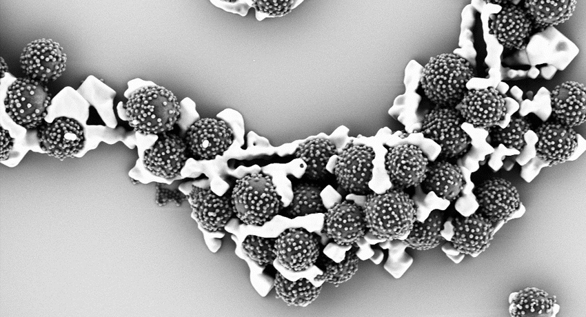
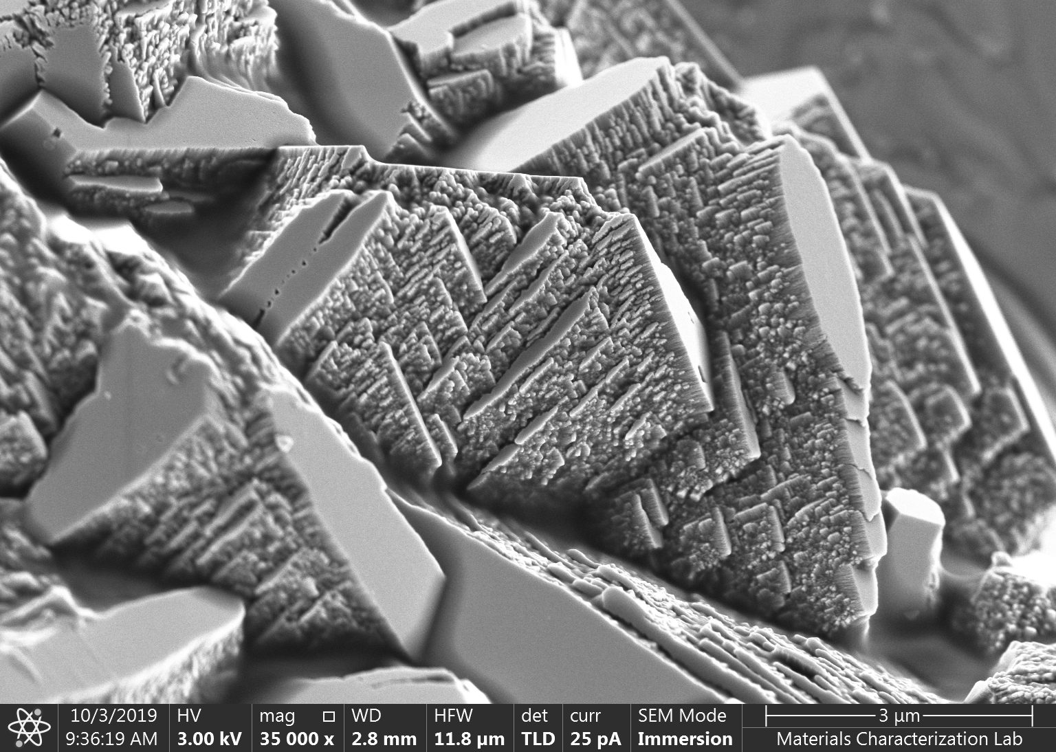
Calcium Carbonate, Verios G4
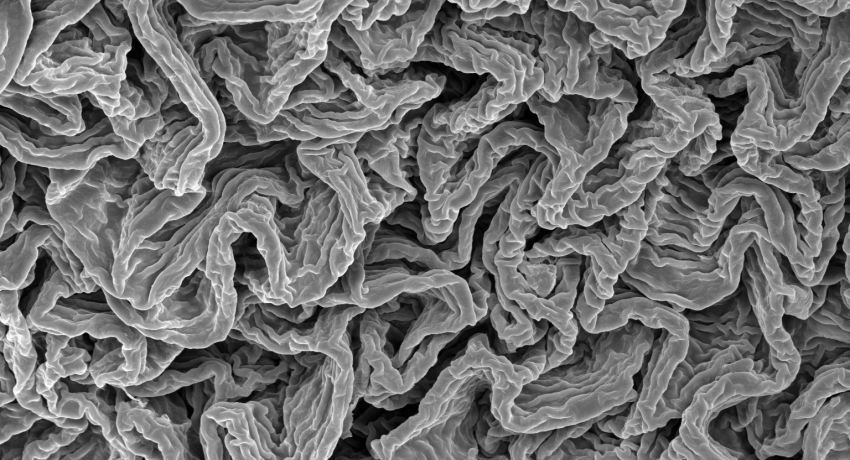
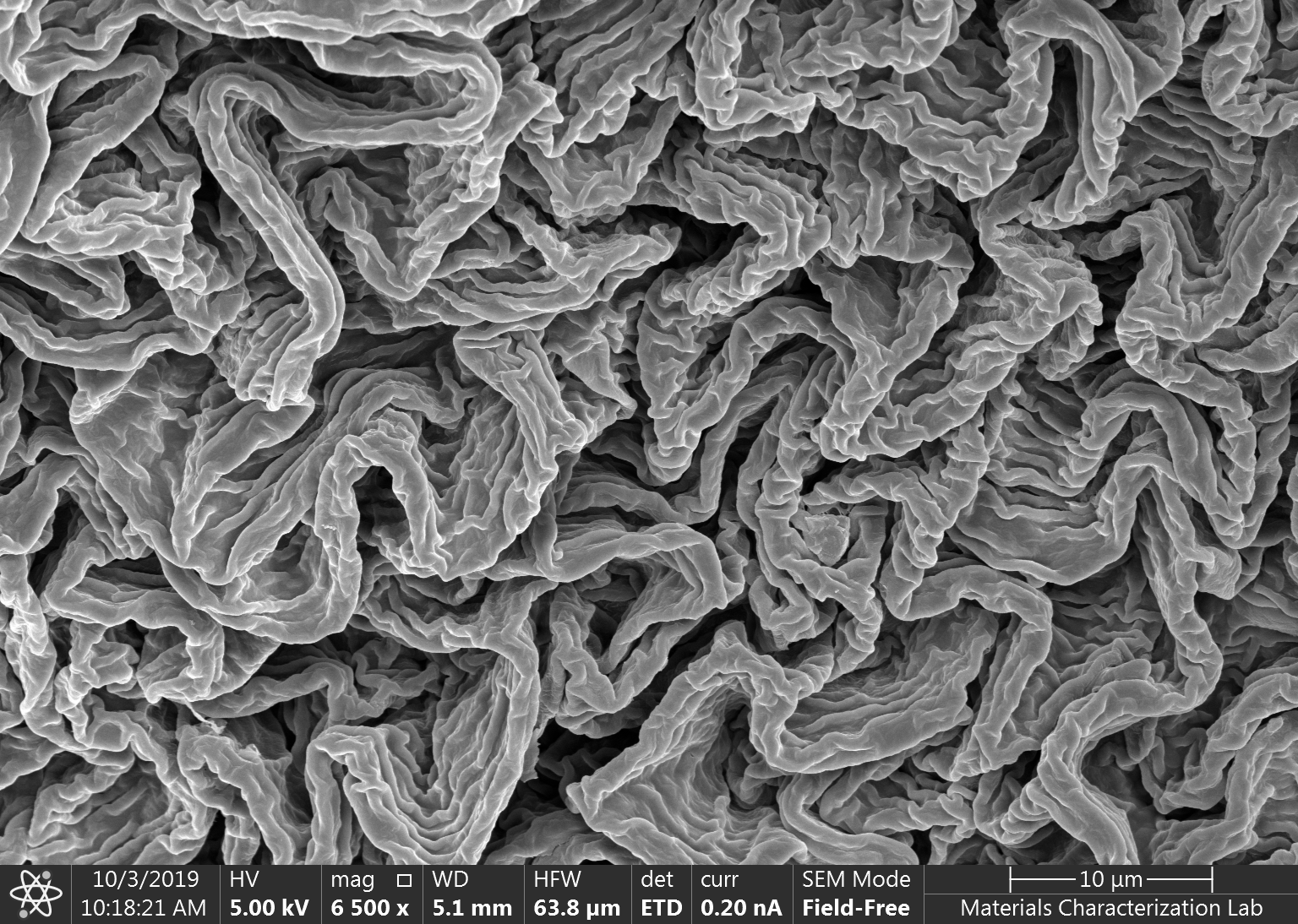
Pollen Surface Morphology, Apreo S
- Secondary electron image for surface morphology.
- Back-scattered imaging to observe elemental contrast.
- Environmental scanning electron microscope mode - Allows for in-situ heating and cooling experiments in the microscope.
- Energy Dispersive Analysis (EDS)
- Electron Backscattered Diffractometry (EBSD)
Sample requirements vary with instrument and analysis desired. Please ask the technical staff about the requirements for your project.
MCL maintains three SEMs. For some of the microscopes, beam deceleration or low vacuum mode can be used to study uncoated insulating and life science specimens. If you need help determining which instrument will best suit your needs please speak with a technical staff member.
| Source | EDS | EBSD | BSE | Other | |
|---|---|---|---|---|---|
| Verios G4 | FEG | X | X | X | Large area mapping |
| Apreo S | FEG | X | X | X | Large area mapping, magnetic samples |
| Axis ChemiSEM | W | X | X | ||
|
Apreo 2S (Maps Mineralogy Suite) |
FEG | X | X | Large area mapping |