
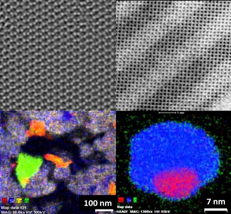
In a transmission electron microscopy (TEM), a thin electron beam transparent specimen (ideally ≤ 100 nm) is exposed to a high-energy (typically 60 - 300 keV) electron beam. Images generally contain contrast that may be due to differences in crystallinity, atomic mass, or thickness variations within the sample. Crystallographic information can also be obtained from diffraction patterns. We can also collect elemental and chemical state maps via analysis of 1) emitted x-rays (Energy Dispersive Spectroscopy – EDS) or 2) the energy loss of electrons that have gone through the specimen (Electron Energy Loss Spectroscopy – EELS). All of our microscopes can also be operated in STEM mode which may be better in some cases for beam sensitive or low contrast samples.
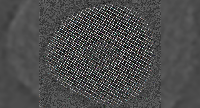
Top: HIgh resolution (N. Alem, V. Gopolan)
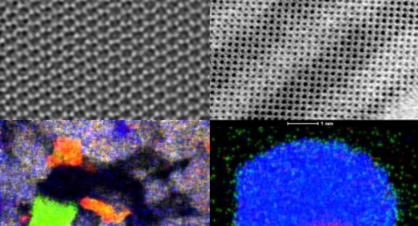
Bottom: EDS maps (N. Abreu, R. Schaak)
- Atomic resolution imaging
- Elemental mapping
- Oxidation state and bonding information
- Crystal structure determination
- Defect and interface analysis
- Grain size and grain boundary analysis
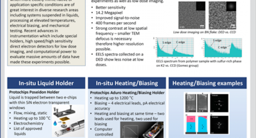
- Low dose imaging
- Cryo TEM
- STEM and TEM tomography
- Lorentz imaging
- Differential Phase Contrast imaging (DPC)
- Gatan 915 cryo-transfer holder (double tilt, EDS compatible)
- In-situ heating and biasing: Protochips Aduro 500
- In-situ liquid and electrochemistry: Protochips Poseidon 510
- Fischione tomography (+/- 70° tilt)
- In-situ PicoIndenter PI 95 holder
| Tecnai G2 | Talos F200C | Talos F200X | Titan3 G2 | |
|---|---|---|---|---|
| Source | LaB6 | X-FEG | X-FEG | X-FEG |
| kV | 80, 200 | 80, 200 | 80, 200 | 60, 80, 200, 300 |
| STEM | X | X | X | X |
| EDS | X | X | Super-X | Super-X |
| EELS/ EFTEM |
X | X | ||
| TEM/STEM Resolution (Å) |
2.4 / 1 | 1.4 / 1.6 | 1.2 / 1.6 | 07. / 0.7 |
| Other | Cryobox | Double Cs corrected, monochromatic |