Electron beam lithography can achieve the smallest features at about 10nm. It is a maskless technique that, like the laser writer, has uses a CAD file for the pattern and can write the pattern directly on the substrate. The electron beam current of Penn State's Raith 5200 is continuously variable with a minimum spotsize of 2nm which is why such small features can be exposed.  The spatial resolution is very good and has control of pitch's on the order of angstroms.

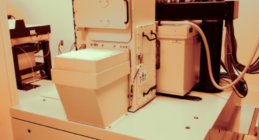
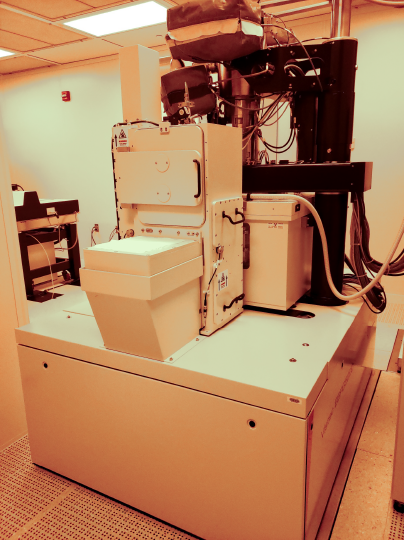
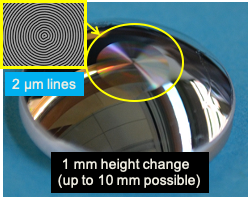
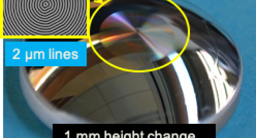
The Raith 5200 and Raith EBPG5200Plus at Penn State have a specialized stage that allows them to expose substrates up to 10 mm thick and with extreme topography and curved surfaces.

Resolution < 10 nm
Overlay < 15 nm

Equipment

Raith EBPG5200 and Raith RBPG5200Plus - Electron Beam Lithography

The Raith EBPG5200 system is used to directly write fine nanometer features in resist. Features as small as 14nm have been achieved. The system has a custom stage with 10mm of Z-height travel for writing curved surfaces as well as parts with extreme topography. The system can handle small parts through 150mm (6 inch) wafers and 5" x 5" mask plates.

The Raith EBPG5200 has been paired with the data (pattern) preparation software Layout Beamer which is easy to use as well as having advanced features such as proximity effect correction.

RAITH EBPG 5200
The RAITH EBPG 5200
e-beam example
Pattern on Curved Surfaces
System: Substrates: Electron Beam Resists Typically Used:
  • 50 & 100kV beam energy
  • Thermal field emission source for a stable high current beam
  • 2nm Gaussian beam size
  • 1mm deflection field size
  • Proximity correction
  • 0.125nm main field resolution
  • 100Mhz beam stepping frequency
  • Stage has 210mm X-Y travel and 10mm Z travel
  • 6Å accuracy on stage location
  • Flexible 2D marker recognition for multi-layer direct write
  • External alignment microscope with height meter
  • Small parts
  • 3" wafers (on small parts holders)
  • 100mm (4 inch) wafers
  • 150mm (6 inch) wafers
  • 5" x 5" mask plates
  • PMMA: high resolution positive resist used for liftoff and sometimes for etching
  • ZEP 520A: high resolution positive resist good for etching and can be used for liftoff of thin metals
  • ZEP 7000-22: moderate resolution, but fast positive resist used primarily for making photomasks
  • MMA-MAA: copolymer for use under PMMA as for the bi-layer liftoff process
  • NEB-31 high resolution, fast negative resist used mostly for etching
  • XR1541/HSQ: ultimate resolution negative resist used for etching mask or as part of device
Lift-off: Pattern for Etch:
  • Single layer liftoff with PMMA
  • Single layer liftoff with ZEP520
  • Bi-Layer liftoff with PMMA & P(MMA/MAA) (co-polymer)
  • Bi-Layer liftoff with XR1541 (HSQ) & PMMA
  • ZEP520
  • NEB31
  • HSQ
Resolution: Stitching Accuracy: Overlay Accuracy: Direct Write Accuracy:
  • 8nm line width @100kV
  • 10nm lines within a 100mm field size ±3nm @100kV
  • 15nm lines within a 250mm field size ±3nm @100kV
  • 20nm lines within a 500mm field size ±3nm @100kV
  • ±15 nm for 100µm main field @100kV
  • ±20 nm for 250µm main field @100kV
  • ±25 nm for 500µm main field @100kV
  • ±25 nm for 500µm main field @50kV
  • ±15 nm for 100µm main field @100kV
  • ±20 nm for 250µm main field @100kV
  • ±30 nm for 500µm main field @100kV
  • ±25 nm for 500µm main field @50kV
  • ±15 nm for 100µm main field @100kV
  • ±20 nm for 250µm main field @100kV
  • ±25 nm for 500µm main field @100kV
  • ±25 nm for 500µm main field @50kV