
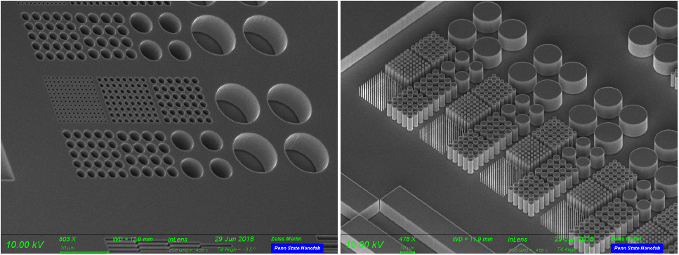
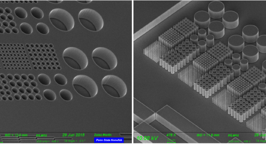
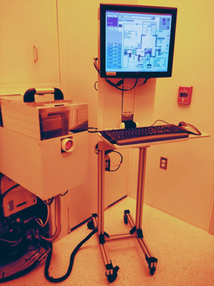
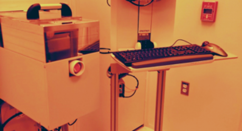
SPTS Deep Silicon Etch Tool
The new SPTS LPX Deep Silicon Etch tool has been installed in the Penn State Materials Research Institute Nanofabrication Laboratory. The system etches silicon using Bosch processing for vertical sidewalls, as well as processing for tapered sidewalls. The electro-static clamping chuck results in better wafer clamping and less wafer bowing compared to mechanical clamping. Etching of features from nano to mm scales can be achieved on 100 mm and 150 mm wafers, smaller substrates can be mounted on a carrier wafer.
For training on this new SPTS LPX Deep Silicon Etch Tool, please contact Guy Lavallee or Shane Miller.
Silicon Etching
SPTS LPX Deep Silicon Etch Tool