Solution found to problem bedeviling semiconductor researchers

Sapphire substrates

By Jamie Oberdick

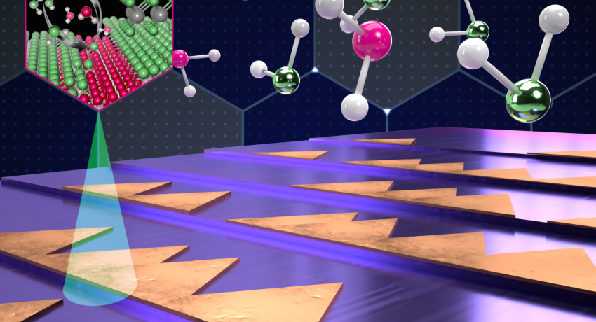
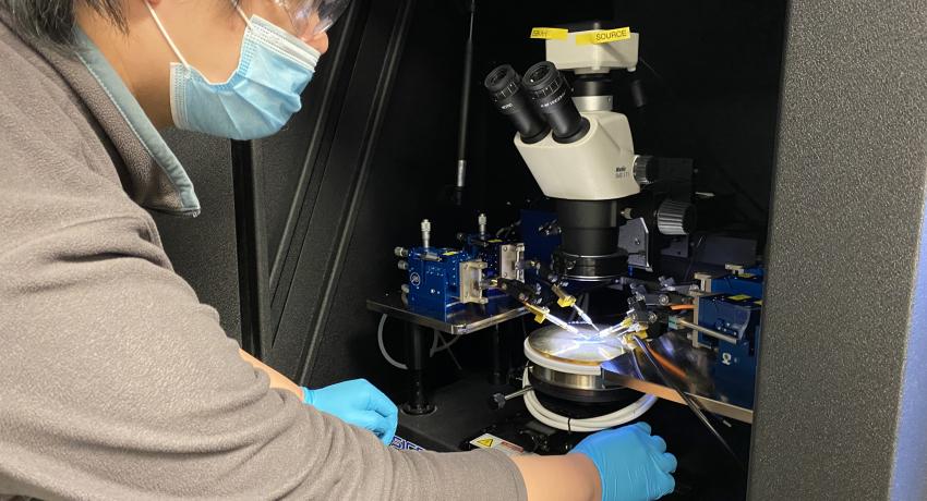
Researchers from the National Science Foundation-sponsored Two-Dimensional Crystal Consortium (2DCC-MIP) - Materials Innovation Platform may have come up with a solution for a bottleneck that has confounded researchers trying to develop high-quality 2D semiconductors for next generation electronics such as Internet of Things (IoT) and artificial intelligence.  

Penn State and onsemi sign MOU to boost silicon carbide research in the U.S.

onsemi and Penn State partnership

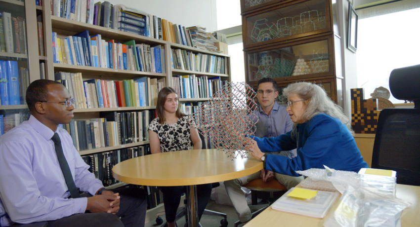
FROM LEFT TO RIGHT: Geanie Umberger, Associate Vice President for Research; Director, Office of Industrial Partnerships, Penn State Sudhir Gopalswamy, Senior Vice President and General Manager, Advanced Solutions Group, onsemi Daniel Lopez, Liang Professor of Electrical Engineering and Computer Science; Director of the Nanofabrication Lab, Penn State Catherine Côté, Vice President and Chief of Staff to the CEO, onsemi Tracy Langkilde, Dean of the Eberly College of Science (front), Penn State Justin Schwartz, Executive Vice President and Provost (back), Penn State Scott Allen, VP of Univ

Semiconductors designed to deliver extreme capabilities

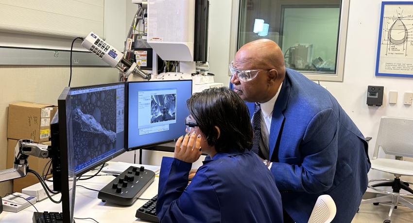
Student examines sample in Chu's lab

By Jamie Oberdick

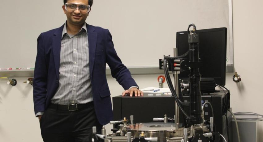
Your cellphone probably would not work very well in space. That is because outer space is full of radiation, and radiation causes defects in electronics that can eventually lead to device failure. You and your cellphone are likely not going to be in outer space anytime soon, but if you are an astronaut relying on electronics to get you to and from space without incident, Rongming Chu’s research may one day be key in keeping you safe.

Packaging is a huge part of the semiconductor puzzle, and Penn State has answers

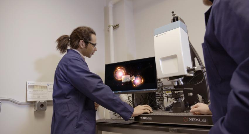
chip packaging

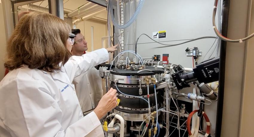
The big news around semiconductors, the factor that drove the CHIPS for America Act, was and is the supply chain. Many in the media focused on the shortages and disruption in the chips supply chain that was caused by the pandemic, and in turn, created big increases in the price of things like automobiles. But there is also another big deal happening with semiconductors that does not get as much attention – packaging.

Growing tomorrow’s semiconductor chips in the materials garden

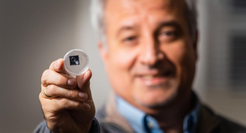
terrones holds a sampl

In some ways, Mauricio Terrones is a gardener. An Evan Pugh University Professor and The Penn State Verne M. Willaman Professor of Physics, Terrones does not grow flowers or vegetables, but instead, one- or few-atom-thick two-dimensional (2D) materials. Specifically, creating materials with specific properties. The first 2D material ever created was graphene, and Terrones was a pioneer in developing 2D materials beyond graphene such as molybdenum disulfide (MoS2) and Tungsten disulfide (WS2). These are layered 2D materials, monolayered, bi-layered, tri-layered or more.