

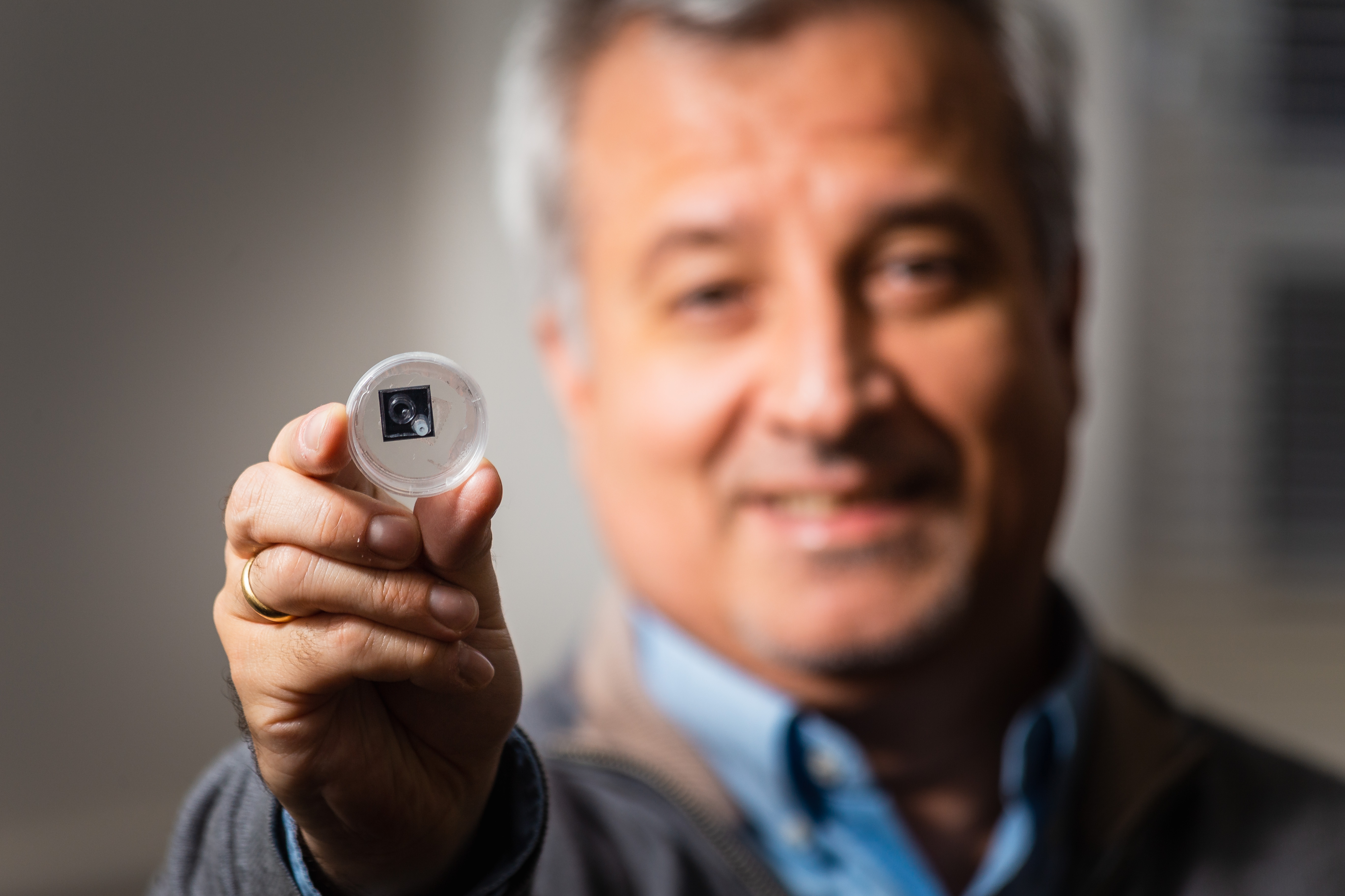
These materials are semiconductors, they are atom thick, and it is important to start thinking about growing these materials in a way that can be applied to semiconductor manufacturing. Credit: Nate Follmer
In some ways, Mauricio Terrones is a gardener. An Evan Pugh University Professor and The Penn State Verne M. Willaman Professor of Physics, Terrones does not grow flowers or vegetables, but instead, one- or few-atom-thick two-dimensional (2D) materials. Specifically, creating materials with specific properties. The first 2D material ever created was graphene, and Terrones was a pioneer in developing 2D materials beyond graphene such as molybdenum disulfide (MoS2) and Tungsten disulfide (WS2). These are layered 2D materials, monolayered, bi-layered, tri-layered or more.
And like with gardening of plants, controlling the growth of 2D materials is important.
“My work involves controlling the growth of the monolayers, bi-layers, and tri-layers of these 2D materials,” Terrones said. “In addition, my group focuses on controlling the crystallinity and the electronic, magnetic and chemical properties of these materials.”
Controlling the growth of these systems can fine-tune them to be efficient semiconductors and improve their performance.
“These materials are semiconductors, they are atom thick, and it is important to start thinking about growing these materials in a way that can be applied to semiconductor manufacturing,” Terrones said. "And do it in a way that we can develop the techniques to quickly characterize them, making them more efficient and unique for the semiconductor industry.”
Potential applications of the materials include development of sensors, including quantum sensors. Quantum sensors detect minute variations in magnetic and electrical fields and are made of quantum materials, which are a class of materials where quantum mechanics play a role in their properties and behavior. Practical applications of these leading-edge sensors are many and varied, from communications technology, neuroimaging, electrical and magnetic field sensors, positioning systems, and microscopy, just to name a few.
“Bringing quantum along would be significant because 2D materials could be used for quantum sensing as well,” Terrones said. “If you have more effective sensors that are faster and detect very tiny amounts of magnetic fields or chemicals, it could open up many different applications.”
Along with growing materials, Terrones also believes it is important to grow collaborations across disciplines.
“For a problem like we have been facing with semiconductors here in America, you need to bring different disciplines together,” Terrones said. “The multidisciplinary convergent sort of framework for research that we have at Penn State is very important for our success. The idea is to bring together not only researchers here at Penn State but companies, other universities, national labs, and so on, bring them all together to first define the problems, and then tackle them collectively in a faster way than we would without the collaboration.”
This approach, Terrones believes, can also apply to educating students that will grow the semiconductor workforce of the future. This includes giving them practical experience.
“From the student perspective, you want students to understand the problems that industry has, and this can be done by internships in companies and/or national labs,” Terrones said. “Once they understand the problem, they can see the research in a different way. They then can move into the field after they leave here and progress faster because they know the problems in and out and understand the fundamentals. I also believe it is important to bring students together from different disciplines so they are speaking the same language and can move forward developing new technologies and move the semiconductor field forward.”
“I think all of this means that we at Penn State have a unique opportunity to help grow the semiconductor industry and make the U.S. self-sufficient,” Terrones added.
This article originally appeared in the Fall 2022 issue of Focus on Materials.