

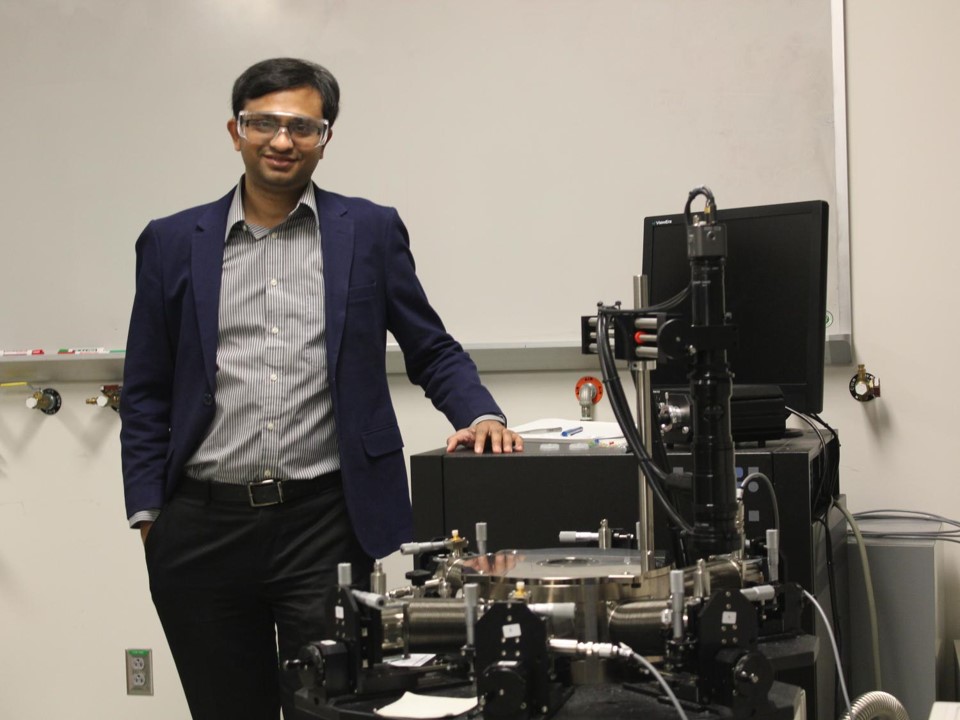
Das group is working on making semiconductor devices, mostly for sensing, computing, storage, and security applications. Credit: Das Group
Silicon has been king for a long time in computer technology. It is the namesake for America’s technology hub, Silicon Valley. However, silicon is nearing its limit as an effective semiconductor material.
Silicon was driven by Moore’s Law, which states that transistors were shrinking so fast that the number that could fit onto a chip was doubling every year, and this in turn would cause computing power to increase and at the same time decrease relative cost. However, silicon can no longer keep up, as performance boosts in new silicon chips are smaller than in previous iterations. Moore’s Law has ended as silicon can no longer accommodate additional transistors, and it would not be good for technology and society in general if we do not have an alternative material ready to replace it. We also need to make the computers more energy-efficient and sustainable since their exploding numbers can be a threat to climate change.
Enter two-dimensional materials as a potential savior, and Penn State researchers such as Saptarshi Das, associate professor of engineering science and mechanics, who are part of the search for the silicon replacement.
“My group is working on making semiconductor devices, mostly for sensing, computing, storage, and security applications,” Das said. “We are trying to really push the technology so that it can be low power and at the same time high performance. To do that we are working on novel materials, and in this particular case, it is a two-dimensional material. The fact that they are ultra-thin makes it possible to scale these devices more aggressively than what you can do with the current silicon technology.”
Das notes that while semiconductors are ubiquitous now, with chips in everything from refrigerators to cars to the phones we always have on hand, they are only going to become even more common. However, Das stresses that these devices of the future must be sustainable and low-power.
"If you think about the total number of semiconductor devices, including now cloud computing, IoT devices, and so on, they are making our life very easy, but at the same time, they're also very energy hungry," Das said. “Each social media post that you make or a WhatsApp image that you send has an energy cost associated with it, while it is negligible for one post or image, when combined at a global scale, we may run into energy challenges. And this is increasing on an exponential trajectory, and it is not going to stop, because we do not want it to stop. It makes our lives so much better and easier. So we need to find solutions that are energy sustainable”
Das’s research group focuses on making the devices that will drive this future, part of what he sees as a wide spectrum of semiconductor research and innovation at Penn State. Another part of this wide spectrum is the National Science Foundation-supported user facility, the Two-Dimensional Crystal Consortium, which works to create the materials needed to make the next generation of semiconductors chips.
“There is natural synergy between the materials folks and the folks like us who are trying to make the next generation of devices,” Das said. “At the same time, we have state-ofthe- art nanofabrication and characterization facilities. Also, once you have the devices you are thinking about, you need to make circuits, architectures systems, and then you have to think about packaging. At Penn State, we have faculty covering this wide spectrum across the layers of our semiconductor ecosystem, and this positions us very strongly in terms of semiconductor research at Penn State.”
Another aspect of the semiconductor puzzle that Das sees Penn State as a contributor is improving the semiconductor workforce development. The recent pandemic-induced chip shortage can be, Das notes, an even worse problem in the future if we fail to develop the critical workforce for semiconductor manufacturing.
“Technological superiority still exists with the U.S. but when it comes to manufacturing semiconductors, it is mostly offshore," Das said. "We have to develop our semiconductor workforce. We have seen during the pandemic, you know, what happens when you have a chip shortage, right? When the production goes down, if we have too much reliability on a very small number of key players, such as the companies like Intel and TSMC, it is not good and shows a need for a plan B.”
Plan B is having more and newer companies coming in and starting to manufacture advanced semiconductors, Das said, and that includes developing an American semiconductor workforce. Das notes that the CHIPS Act is a good first step towards this “Plan B.”
“I think universities like Penn State and the existing semiconductor industry have to partner up because I don't think universities can alone do it, nor can the semiconductor industry,” Das said. "There is an urgent need, so we need to get started as soon as possible on this thing, otherwise, it's going to be too late.”
This article originally appeared in the Fall 2022 issue of Focus on Materials.