

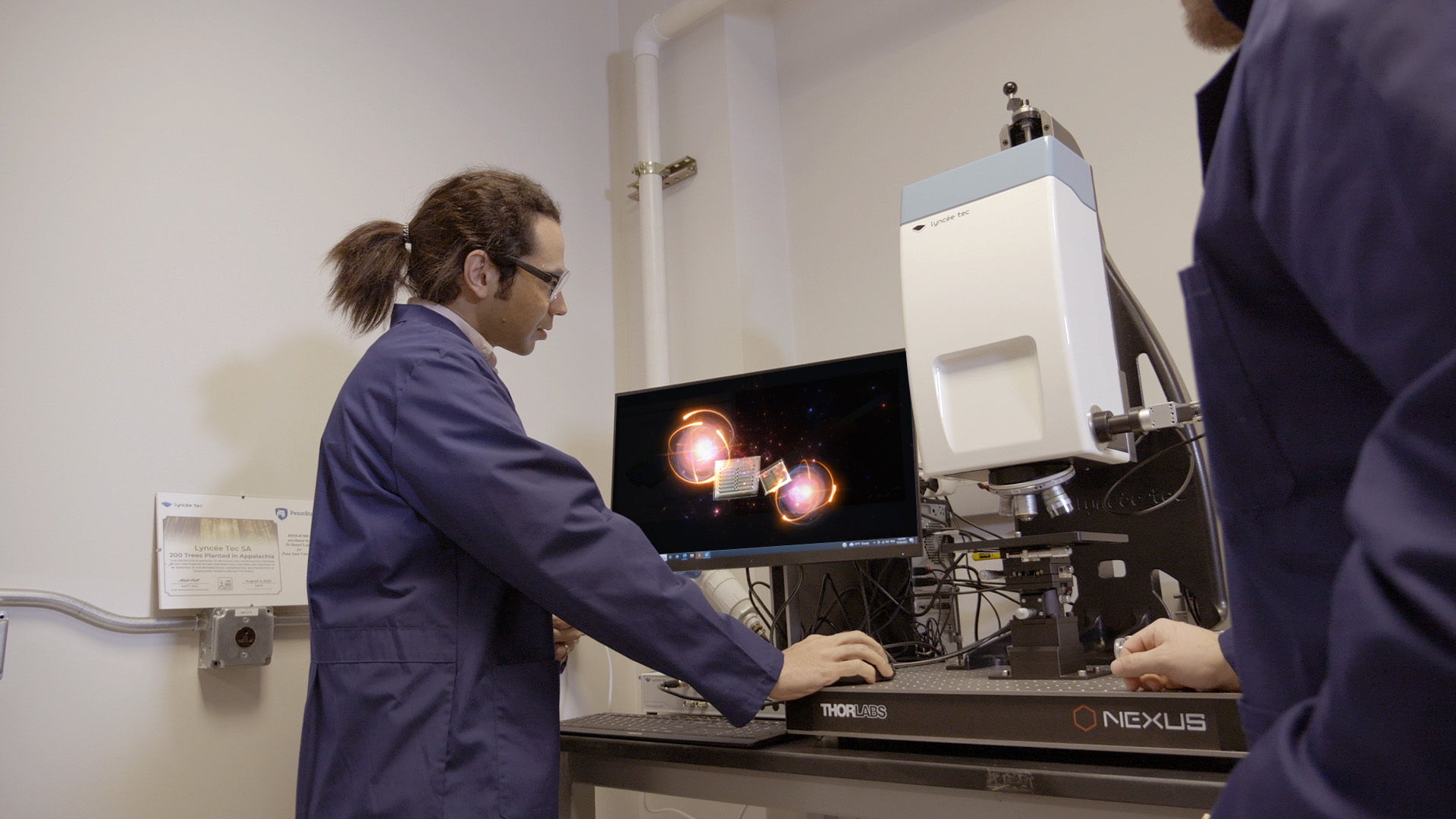
Prof. Daniel Lopez research group in the lab in the Millennium Science Complex. Credit: Corey Beasley and Jennifer M. McCann
The big news around semiconductors, the factor that drove the CHIPS for America Act, was and is the supply chain. Many in the media focused on the shortages and disruption in the chips supply chain that was caused by the pandemic, and in turn, created big increases in the price of things like automobiles. But there is also another big deal happening with semiconductors that does not get as much attention – packaging.
Penn State’s material researchers have been working in these areas for a long time, and soon these efforts will get a boost. Penn State has an incoming head of the Department of Electrical Engineering, Madhavan Swaminathan, who will enhance Penn State’s efforts in packaging and supply chain research. Swaminathan comes to Penn State from Georgia Tech, where he was the director of the 3D Systems Packaging Research Center, the largest academic center of its kind in the world.
Packaging used to be considered a relatively non-essential part of semiconductor design but no longer. Packaging affects power, performance, cost, reliability, and the basic functionality of chips. It is the container that holds the semiconductor, protects the die (unpackaged, bare chip), connects the chip to a motherboard and/or other chips, and can be used to remove heat.
“These chips have to be packaged for several reasons,” Swaminathan said. “One of them is for the chips to communicate with each other and to be able to communicate with the external world. Semiconductor packaging has come into the forefront when it comes to semiconductor chips today. In fact, a major area of investment in the CHIPS Act is semiconductor packaging.”
Swaminathan's research is on applications such as wireless communications, both 5G and beyond; high-performance computing for artificial intelligence; and electronics that must operate in harsh environments such as in an automobile or outer space. In assessing Penn State’s capabilities with semiconductors, he looks at how the University fits into the semiconductor “ecosystem.”
“There are several layers associated with semiconductors,” Swaminathan said. “One of them is the area of the device. And then these devices must come together in the form of circuits. And those circuits then are integrated within a chip and the chip needs to be packaged and ultimately the chips are connected to each other to form a system. So that is the ecosystem that one needs and if you look at Penn State, there are several elements of this already there.”
Swaminathan will join the work already being done with packaging at Penn State and help to plan the next steps for packaging research, such as exploring new forms of packaging through work with the Materials Research Institute. This includes quantum computing packaging, which uses glass materials, for example. Such work will require an interdisciplinary effort.
"As the department head, I hope to expand quite a bit so that several faculty members both within electrical engineering, as well as other departments, get involved in packaging research,” Swaminathan said. “Semiconductor packaging is highly multidisciplinary, where for example we have faculty working from mechanical engineering, looking into stress-related issues centered around reliability. Then you have people from material science and engineering looking into areas related to 2D materials, thermal interface materials, and things of that nature. And then you have electrical engineers designing the system package as well as developing fabrication processes working with other disciplines.”
To achieve this, part of Swaminathan’s plan is to develop a packaging research center at Penn State, like the one he directed at Georgia Tech.
“The hope is that we are able to create a center at Penn State that is able to come up with capabilities that are complementary to other capabilities that are available within the United States and other universities,” Swaminathan said. “We can then take the leadership role when it comes to developing advanced semiconductor packaging that is necessary in the future.”
Swaminathan also envisions Penn State playing a role in semiconductor job development. He notes that while people think of technology jobs in the context of someone graduating from the Northeast and moving to the Silicon Valley, technology jobs can be a boon for Pennsylvania and the surrounding region. He points to Intel setting up a plant in Ohio.
“It's really people from places like Ohio, Indiana, Pennsylvania, and others who will be a significant part of the semiconductor workforce and ecosystem,” Swaminathan said. “There are people who want to stay near their families for work. It is very, very important to them. So, my belief is that soon, the Mid-Atlantic, the Midwest, these areas are going to grow quite a bit as far as semiconductor-related jobs, which is exceptionally good for these local economies.
This article originally appeared in the Fall 2022 issue of Focus on Materials.