

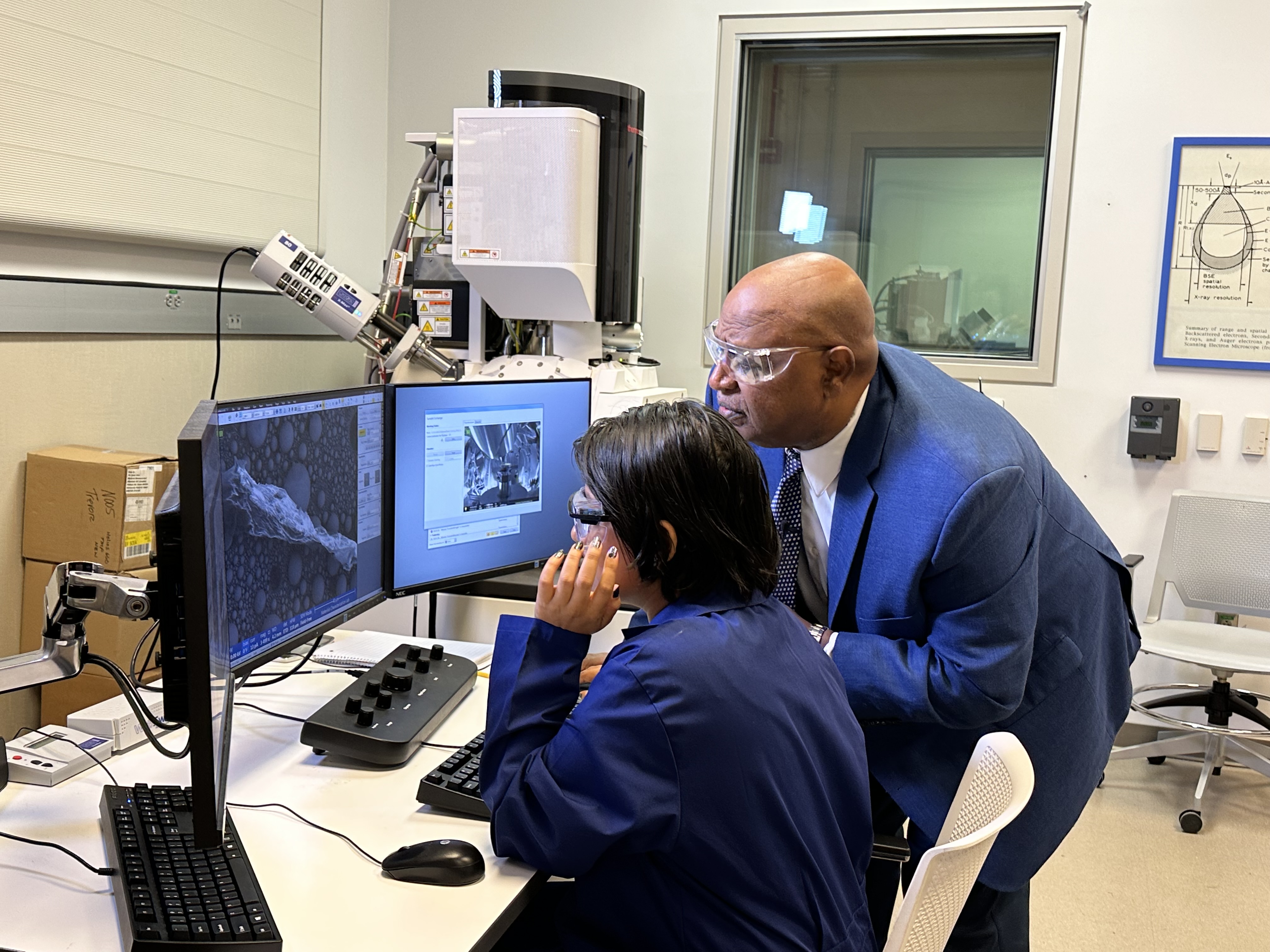
The CNEU works with industry, Pennsylvania four-year universities, Pennsylvania community colleges, and other two-year-degree granting institutions to create degree programs related to semiconductor processing and nanofabrication.. Credit: Jennifer M. McCann
By Jamie Oberdick
A key to America's future semiconductor success story will be building a skilled workforce, a well-prepared set of workers to address the needs of the chips industry. Workforce development is an essential part of the Chips and Science Act, designed to meet the needs of the semiconductor industry.
As if they had a crystal ball to see the CHIPS and Science Act coming, Penn State is on it, and has been for a while. Founded in 1998, Penn State’s Center for Nanotechnology Education and Utilization (CNEU) is an important driver of semiconductor workforce education. The CNEU works with industry, Pennsylvania four-year universities, Pennsylvania community colleges, and other two-year-degree granting institutions to create degree programs related to semiconductor processing and nanofabrication. According to Osama Awadelkarim, UNESCO Chair Professor and director of the CNEU, this overall effort has evolved into the Pennsylvania Nanofabrication Manufacturing Technology Partnership (PA NMT). The PA NMT is a broad micro- and nano-scale fabrication, synthesis, and characterization educational experience addressing the career needs of students and the technician needs of a wide spectrum of semiconductor-based industries.
The PA NMT partner institutions receive access to resources they would not ordinarily have.
“This is a very expensive kind of training, as it takes resources such as cleanrooms, very skilled personnel, very expensive types of lab equipment, and so on,” Awadelkarim said. “Community colleges in Pennsylvania don’t have these, in fact, many four-year universities do not. So the idea is to make Penn State’s facilities accessible to those institutions who do not have these resources and enable the community colleges and four-year universities map out their own nanomanufacturing education program.”
These institutions create their own nanomanufacturing program that includes an 18-credit capstone semester, which is designed with industry partners via the CNEU Industry Advisory Board.
“The capstone is a hands-on immersion for students in micro- and nano-scale fabrication and characterization over 12 weeks taught in CNEU’s teaching cleanroom at Penn State’s University Park campus,” Awadelkarim said. “It is such a great opportunity for students from smaller institutions to take advantage of, this nanofabrication infrastructure of equipment, staff, and faculty resources.”
The PA NMT was funded by the state of Pennsylvania for a number of years and incorporates more than 40 Pennsylvania community colleges and four-year universities, with approximately 1,000 students graduating from the program. To meet the workforce needs of the semiconductor industry, Awadelkarim notes that it is vital to draw significant number of skilled workers from female and underrepresented ethnic populations, along with veterans.
“So, since 2018, we have collaborated with historically black colleges and universities, HBCUs, and Hispanic serving institutions,” Awadelkarim said. “To date, we have trained 45 students from these groups at CNEU facilities along with about 160 trained remotely. For veterans, we have begun to offer the Nanomanufacturing Certificate Program to veterans recruited from around Norfolk, Virginia. And now, thanks to a $4.7 million grant from the NSF, this is going to be expanded to include Navy, Air Force, Marines, and Army bases in San Diego, Atlanta, and Phoenix.”
This work has established Penn State as a leader in micro- and nanomanufacturing education and workforce, so much so the NSF created the Advanced Technological Education (ATE) Center for Nanotechnology Applications and Career Knowledge (NACK) at CNEU to mimic the PA NMT model nationwide. This extends the benefits realized by community and technical colleges in Pennsylvania to potentially a national scale, enabling them to provide associate degree level micro- and nanofabrication education. NACK and CNEU have helped in creating more than 10 resource-sharing partnerships that provide the workforce training the United States must have for semiconductor competitiveness.
Along with helping to train students, CNEU also offers the Nanomanufacturing Professional Development (NPD) program for nanomanufacturing-related training of faculty in community colleges and four-year universities as well as incumbent semiconductor industry workers. The NPD began with an in-person training format and was then adapted to web-based live-streaming and fully interactive delivery mode. These were supported by NSF grants.
“The live-streaming delivery mode of the NPD has proven to be very effective in reducing cost and in making the NPD accessible to a much larger group of educators and faculty,” Awadelkarim said. “More than 1,800 educators and industry people have completed the NPD workshops.”
Yet another program to promote semiconductor workforce is the Remotely Accessible Instruments for Nanotechnology (RAIN) service, which offers web access to cutting-edge nanocharacterization tools at 28 partnering institutions in the RAIN Network. RAIN has provided close to 600 remote access sessions to more than 11,000 students.
All of these different initiatives have given Penn State a leadership role in developing strong technical workforce, a key element of the CHIPS and Science Act.
“We’ve expanded what we’ve done in CNEU to a national level,” Awadelkarim said. “So, in other words, we’ve already, even before the CHIPS and Science Act, have been active in semiconductor workforce development. For more than 20 years, we have done this, to the point where if you go to a community college, there is a good chance that they know about CNEU’s work in nanotechnology workforce development because they’ve used our resources.”
This article originally appeared in the Fall 2022 issue of Focus on Materials.