

MCL maintains multiple sputter coaters to enable the preparation of specimens for available electrical characterization and microscopy techniques.
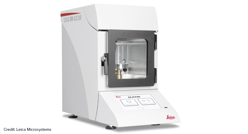
| System | Quorum Q150R Sputter Coater | Leica Sputter Coater | Emitech Sputter Coater |
|---|---|---|---|
| Practical Sample Size | ≤ 50 mm Dia. x 12 mm H | ≤ 30 mm Dia. x < 50 mm H | ≤ 50 mm Dia. x < 5 mm H |
| Sputter Metals | Gold Silver Platinum |
Carbon Iridium |
Iridium |
| Common Use | Bulk pellets and thin film for electrical characterization imaging in SEM | Sputter coat thin layer of conductive material for SEM, TEM, and EPMA imaging | Sputter coat thin layer of conductive material for SEM and TEM imaging |
| Deposition Thickness Range | 5 to 100s nm | 1nm to 40 nm | 1 nm to 20 nm |
| Vacuum Type | Rough pump | Turbo pump | Turbo pump |
| Technical Expert | Jeff Long | Julie Anderson and Wes Auker | Julie Anderson and Wes Auker |