This can be for any year.

Scalable CMOS back-end-of-line-compatible AlScN/2D channel ferroelectric field-effect transistors
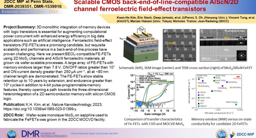
Scalable CMOS back-end-of-line-compatible AlScN/2D channel ferroelectric field-effect transistors

3D monolithic integration of memory devices with logic transistors is essential for augmenting computational power concurrent with enhanced energy efficiency in big data applications such as artificial intelligence. Ferroelectric field-effect transistors (FE-FETs) are a promising candidate, but requisite scalability and performance in a back-end-of-line process have proven challenging. Here we present BEOL-compatible FE-FETs using 2D MoS2 channels and AlScN ferroelectric materials, all grown via wafer-scalable processes.
Quantifying interfacial energetics of 2D semiconductor electrodes using in situ spectroelectrochemistry and many-body theory

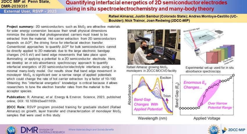
Quantifying interfacial energetics of 2D semiconductor electrodes using in situ spectroelectrochemistry and many-body theory

2D semiconductors such as MoS2 are attractive materials for solar energy conversion because their small physical dimensions minimize the distance that photogenerated carriers must travel to be extracted from the material. Hot carrier extraction from 2D semiconductors depends on ΔG°′, the driving force for interfacial electron transfer.

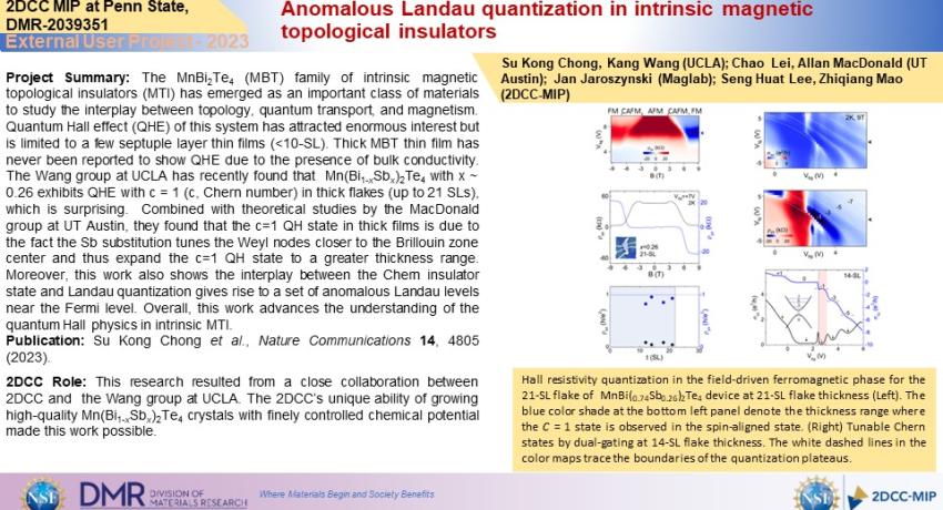
Anomalous Landau quantization in intrinsic magnetic topological insulators

Anomalous Landau quantization in intrinsic magnetic topological insulators

The MnBi2Te4 (MBT) family of intrinsic magnetic topological insulators (MTI) has emerged as an important class of materials to study the interplay between topology, quantum transport, and magnetism. Quantum Hall effect (QHE) of this system has attracted enormous interest but is limited to a few septuple layer thin films (<10-SL). Thick MBT thin film has never been reported to show QHE due to the presence of bulk conductivity.

Modulation Effect of Substrate Interactions on Nucleation and Growth of MoS2 on Silica

Modulation Effect of Substrate Interactions on Nucleation and Growth of MoS2 on Silica

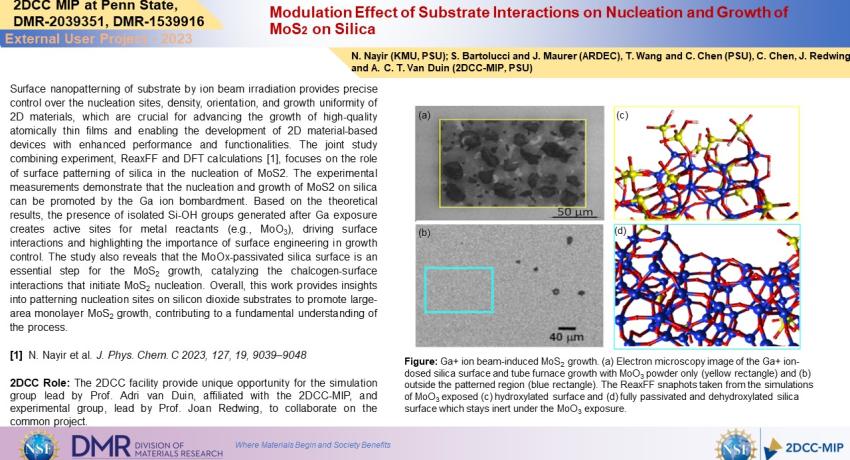
Surface nanopatterning of substrate by ion beam irradiation provides precise control over the nucleation sites, density, orientation, and growth uniformity of 2D materials, which are crucial for advancing the growth of high-quality atomically thin films and enabling the development of 2D material-based devices with enhanced performance and functionalities. The joint study combining experiment, ReaxFF and DFT calculations [1], focuses on the role of surface patterning of silica in the nucleation of MoS2.

Stabilizing far-from-equilibrium (Mo,Ti)S2 thin films by metal sulfurization at reduced temperature

Stabilizing far-from-equilibrium (Mo,Ti)S2 thin films by metal sulfurization at reduced temperature

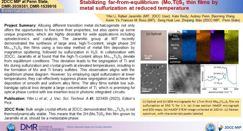
Alloying different transition metal dichalcogenides not only offers the opportunities to fine-tune their properties, but also opens up some unique properties, which are highly desirable for wide applications including optoelectronics and catalysis. The Jaramillo group at MIT recently demonstrated the synthesis of large area, high-Ti-content, single phase 2H Mo1−xTixS2 thin films using a two-step method of metal film deposition by magnetron sputtering, followed by sulfurization in H2S. In collaboration with 2DCC, Jaramillo et al.

Self-limiting stoichiometry in SnSe thin films

Self-limiting stoichiometry in SnSe thin films

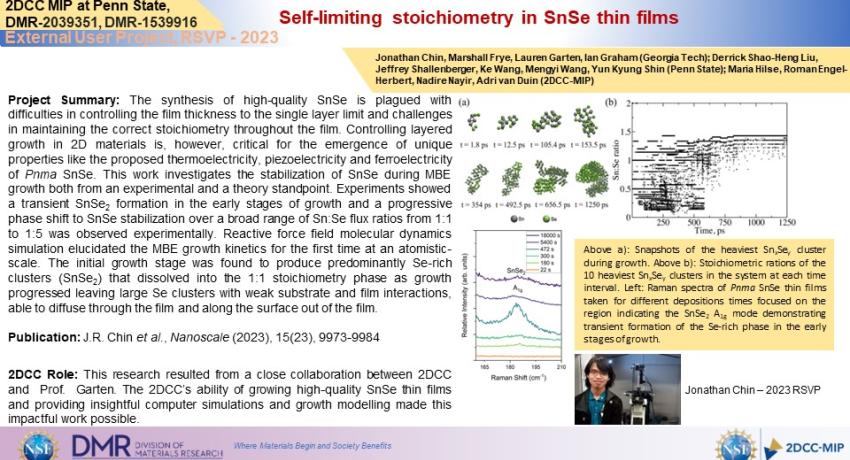
The synthesis of high-quality SnSe is plagued with difficulties in controlling the film thickness to the single layer limit and challenges in maintaining the correct stoichiometry throughout the film. Controlling layered growth in 2D materials is, however, critical for the emergence of unique properties like the proposed thermoelectricity, piezoelectricity, and ferroelectricity of Pnma SnSe. This work investigates the stabilization of SnSe during MBE growth both from an experimental and a theory standpoint.

Where does the current flow in a quantum anomalous Hall insulator?

Where does the current flow in a quantum anomalous Hall insulator?

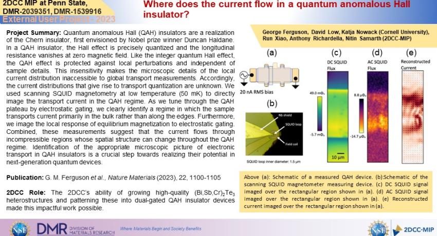
Quantum anomalous Hall (QAH) insulators are a realization of the Chern insulator, first envisioned by Nobel prize winner Duncan Haldane. In a QAH insulator, the Hall effect is precisely quantized and the longitudinal resistance vanishes at zero magnetic field. Like the integer quantum Hall effect, the QAH effect is protected against local perturbations and independent of sample details. This insensitivity makes the microscopic details of the local current distribution inaccessible to global transport measurements.

Elucidating the Mechanism of Large Phosphate Molecule Intercalation Through Graphene-Substrate Heterointerfaces

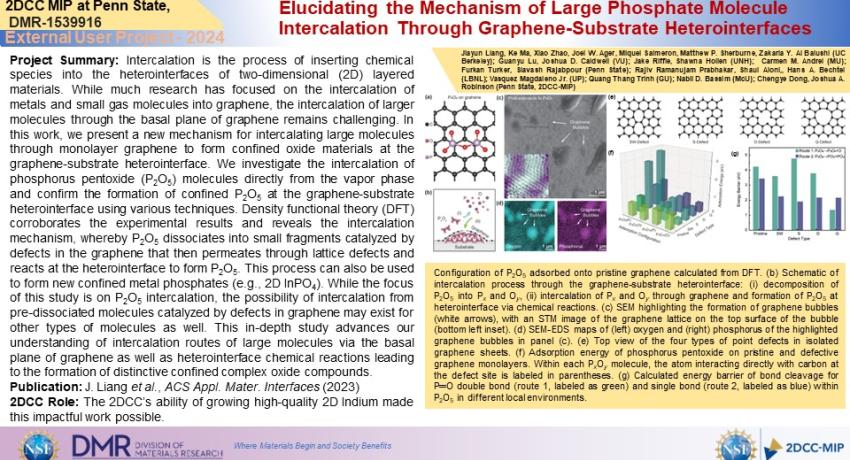
Elucidating the Mechanism of Large Phosphate Molecule Intercalation Through Graphene-Substrate Heterointerfaces

Intercalation is the process of inserting chemical species into the heterointerfaces of two-dimensional (2D) layered materials. While much research has focused on the intercalation of metals and small gas molecules into graphene, the intercalation of larger molecules through the basal plane of graphene remains challenging. In this work, we present a new mechanism for intercalating large molecules through monolayer graphene to form confined oxide materials at the graphene-substrate heterointerface.

Watching (De)Intercalation of 2D Metals in Epitaxial Graphene: Insight into the Role of Defects​

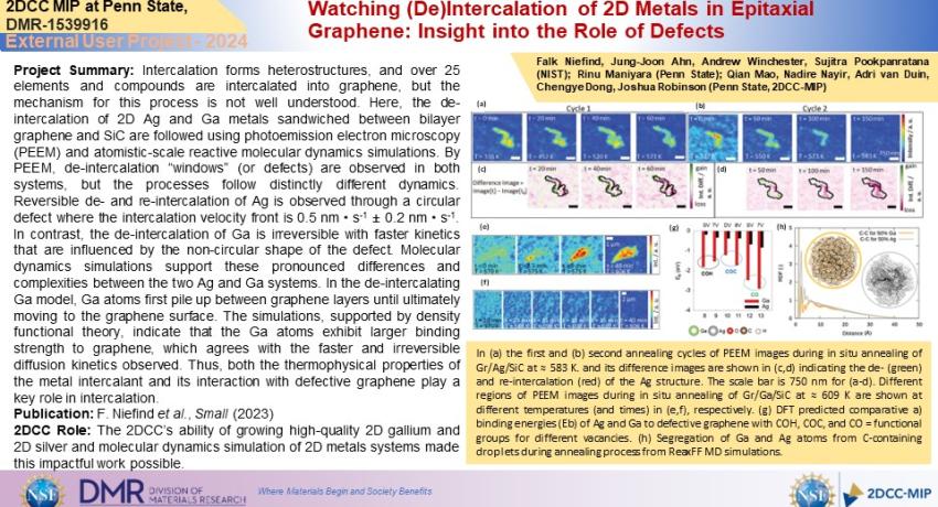
Watching (De)Intercalation of 2D Metals in Epitaxial Graphene: Insight into the Role of Defects​

Intercalation forms heterostructures, and over 25 elements and compounds are intercalated into graphene, but the mechanism for this process is not well understood. Here, the de-intercalation of 2D Ag and Ga metals sandwiched between bilayer graphene and SiC are followed using photoemission electron microscopy (PEEM) and atomistic-scale reactive molecular dynamics simulations. By PEEM, de-intercalation “windows” (or defects) are observed in both systems, but the processes follow distinctly different dynamics.