This can be for any year.

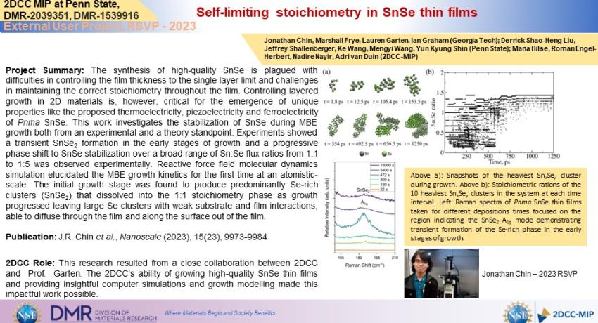
Light-driven C-H activation mediated by 2D transition metal dichalcogenides

Light-driven C-H activation mediated by 2D transition metal dichalcogenides

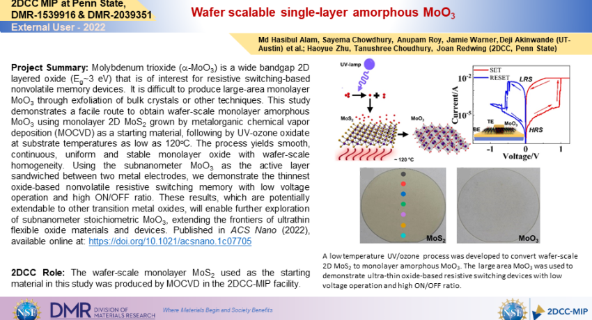
Project Summary: The activation and functionalization of C-H bonds enables new synthetic routes for functional molecules. Since C-H bonds are thermodynamically strong, metal catalysts such as Pd, Co, Au, etc. in combination with a zeolite or metalorganic framework are typically employed. Here we report light-driven C-H activation in complex organic molecules mediated by 2D transition metal dichalcogenides (TMDs). The process involves efficient hydrogen adsorption and a lowered energy barrier of C-C coupling mediated by TMDs.

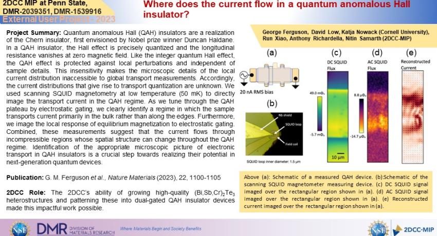
Distinguishing surface and bulk electromagnetism via their dynamics in an intrinsic magnetic topological insulator

Distinguishing surface and bulk electromagnetism via their dynamics in an intrinsic magnetic topological insulator

Project Summary: The indirect exchange interaction between local magnetic moments via surface electrons has been long
predicted to bolster the surface ferromagnetism in magnetic topological insulators (MTIs), which facilitates the quantum anomalous

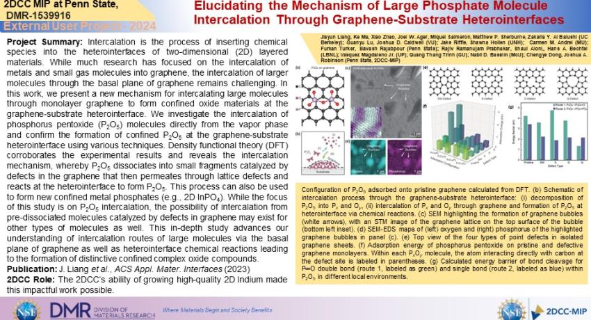
Confinement of Excited State in Two-Dimensional In-Plane Quantum Heterostructures

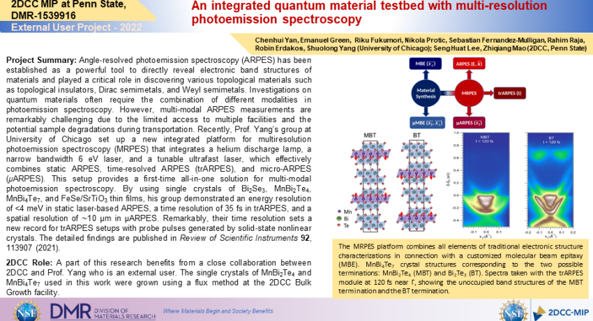
Project Summary: 2D semiconductors are promising candidates for quantum information processes and offer the possibility of achieving in-plane exciton confinement, similar to zero-dimensional quantum dots, with intriguing optical and electronic properties via strain or composition engineering. However, realizing such laterally confined 2D dots and systematically controlling their size is challenging. Here, we report the observation of lateral confinement of excitons in in-plane MoSe2quantum dots (~15-60 nm w

Project Summary: 2D semiconductors are promising candidates for quantum information processes and offer the possibility of achieving in-plane exciton confinement, similar to zero-dimensional quantum dots, with intriguing optical and electronic properties via strain or composition engineering. However, realizing such laterally confined 2D dots and systematically controlling their size is challenging.

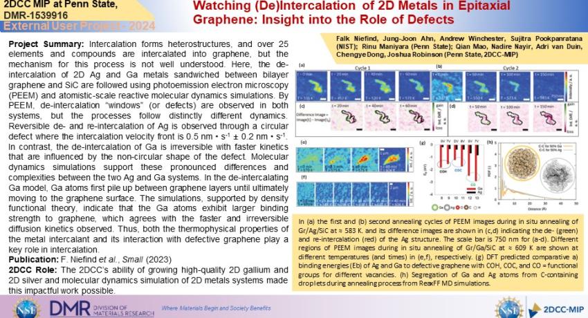
Three-dimensional integration of two-dimensional field-effect transistors

Three-dimensional integration of two-dimensional field-effect transistors

With the escalating costs of developing and manufacturing integrated circuit (IC) chips, methods to vertically stack devices are being thoroughly explored. While silicon-based 3D ICs have been achieved using innovative packaging solutions, there has been limited exploration of emerging nanomaterials, such as 2D Transition metal dichalcogenides (TMDs), for a monolithic 3D chip.

Wafer-scale transition metal dichalcogenides enable large area 2D electronics and optoelectronics

Wafer-scale transition metal dichalcogenides enable large area 2D electronics and optoelectronics

Ultra-thin 2D semiconductors based on monolayer transition metal dichalcogenides (TMDs) are seen as potential candidates for future generation electronic and optoelectronic devices for energy efficient computing and sensing for applications such as Internet-of-Things and artificial intelligence. Wafer-scale epitaxial TMD monolayers grown by metalorganic chemical vapor deposition (MOCVD) in the 2D Crystal Consortium Materials Innovation Platform facility can be readily transferred from the growth substrate for heterogeneous integration enabling large area device demonstrations.

Efficient thermally generation of a spin current in a topological insulator

Efficient thermally generation of a spin current in a topological insulator

The canonical topological insulator Bi2Se3 has played a central role in the development of ‘topological spintronics,’ a framework that seeks to exploit the inherent spin-momentum correlation in helical Dirac surface states for spin transport devices that could be used for non-volatile magnetic random access memory. Prior experiments have focused on studying efficient interconversion between spin current and charge current in devices that interface a topological insulator with a ferromagnet.

Low-Frequency Raman Study of Large-Area Twisted Bilayers of WS_2 Stacked by an Etchant-Free Transfer Method

Low-Frequency Raman Study of Large-Area Twisted Bilayers of 𝐖𝐒_𝟐 Stacked by an Etchant-Free Transfer Method

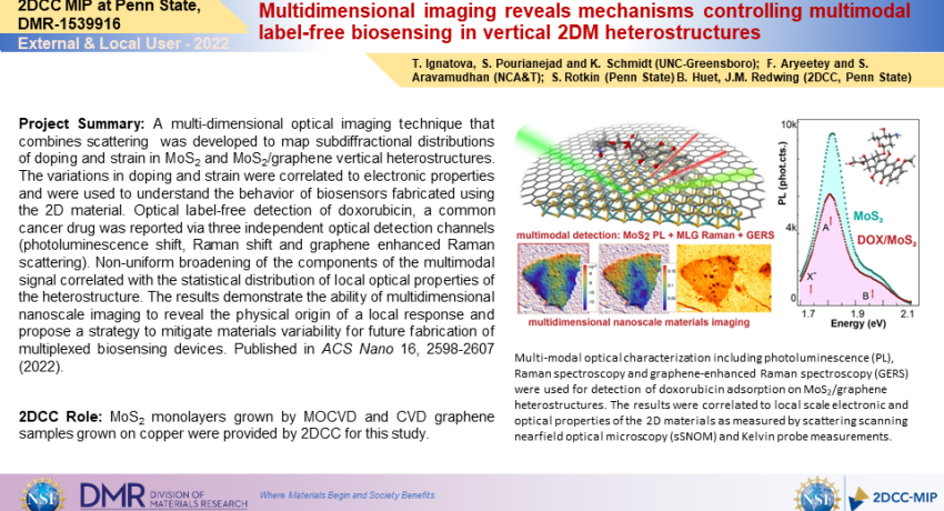
Transition metal dichalcogenides have strong intra-covalent bonding. When stacked in multilayers, weak van der Waals interactions dominate interlayer mechanical coupling and influence their lattice vibrations. In this work, we developed an efficient transfer method for fabricating bilayers of WS2 with a controlled twist angle. We investigated the evolution of interlayer and moiré phonons, and photoluminescence bandgap depending on the twist angle.

Nonvolatile Memristive Effect in Few Layer CrI3 Driven by Electrostatic Gating

Nonvolatile Memristive Effect in Few Layer CrI3 Driven by Electrostatic Gating

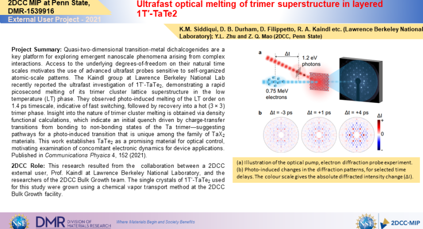
The potential of memristive devices for applications in nonvolatile memory and neuromorphic computing has sparked considerable interest, particularly in exploring memristive effects in two-dimensional (2D) magnetic materials. However, the progress in developing nonvolatile, magnetic field-free memristive devices using 2D magnets has been limited. By fabricating CrI3-based tunnel junctions, the Tian group at University of Wyoming has recently demonstrated the realization of electrostatic-gating-induced nonvolatile memristive effect. Tian et al.