This can be for any year.

Wafer scalable single-layer amorphous molybdenum trioxide
Wafer scalable single-layer amorphous MoO3

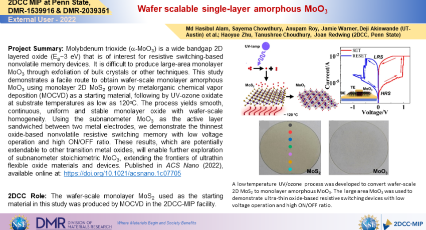
Project Summary: Molybdenum trioxide (a-MoO3) is a wide bandgap 2D layered oxide (Eg~3 eV) that is of interest for resistive switching-based nonvolatile memory devices.  It is difficult to produce large-area monolayer MoO3 through exfoliation of bulk crystals or other techniques. This study demonstrates a facile route to obtain wafer-scale monolayer amorphous MoO3 using monolayer 2D MoS2 grown by metalorganic chemical vapor deposition (MOCVD) as a starting material, following by UV-ozone oxidate at substrate temperatures as low as 120oC.
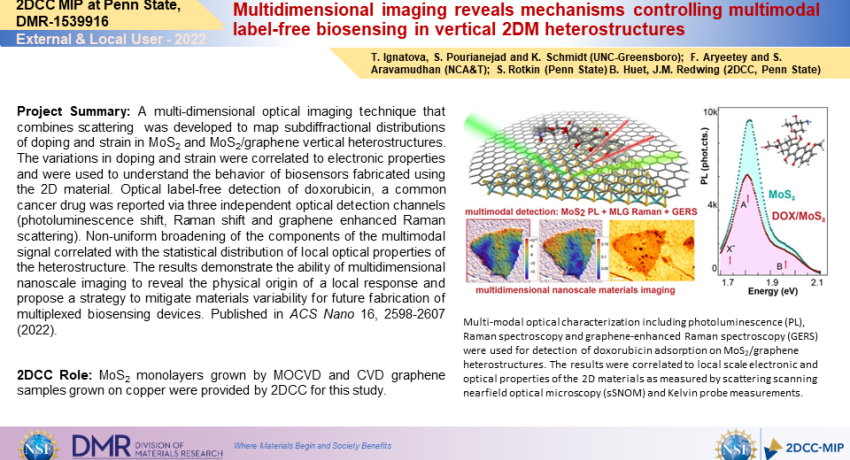
Multidimensional imaging reveals mechanisms controlling multimodal label-free biosensing in vertical 2DM heterostructures

Multidimensional imaging reveals mechanisms controlling multimodal label-free biosensing in vertical 2DM heterostructures

Project Summary: A multi-dimensional optical imaging technique that combines scattering  was developed to map subdiffractional distributions of doping and strain in MoS2 and MoS2/graphene vertical heterostructures.

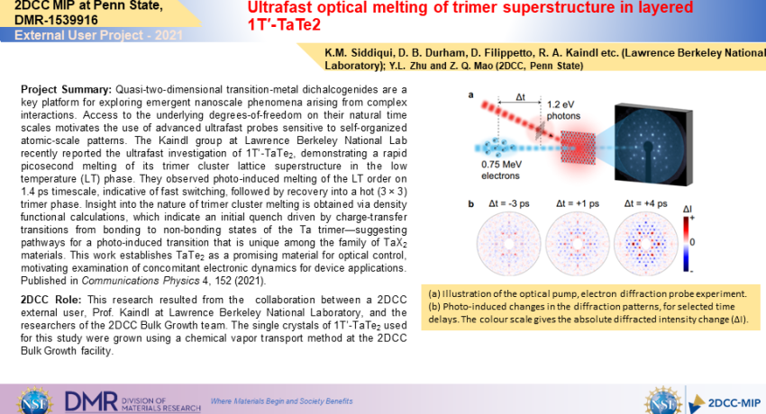
Ultrafast optical melting of trimer superstructure in layered 1T′-TaTe2

Ultrafast optical melting of trimer superstructure in layered 1T′-TaTe2

Project Summary: Quasi-two-dimensional transition-metal dichalcogenides are a key platform for exploring emergent nanoscale phenomena arising from complex interactions. Access to the underlying degrees-of-freedom on their natural time scales motivates the use of advanced ultrafast probes sensitive to self-organized atomic-scale patterns.

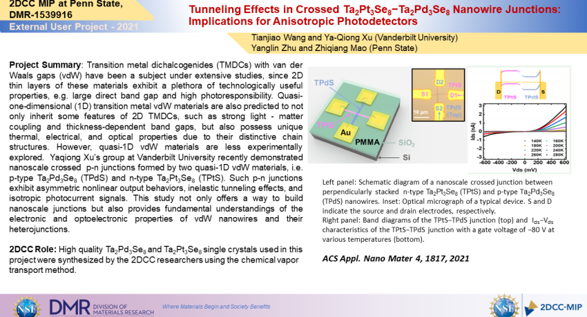
Tunneling Effects in Crossed Ta2Pt3Se8−Ta2Pd3Se8 Nanowire Junctions: Implications for Anisotropic Photodetectors

Tunneling Effects in Crossed Ta2Pt3Se8−Ta2Pd3Se8 Nanowire Junctions: Implications for Anisotropic Photodetectors

Project Summary: Transition metal dichalcogenides (TMDCs) with van der Waals gaps (vdW) have been a subject under extensive studies, since 2D thin layers of these materials exhibit a plethora of technologically useful properties, e.g. large direct band gap and high

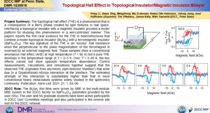
Topological Hall Effect in Topological Insulator/Magnetic Insulator Bilayer

Topological Hall Effect in Topological Insulator/Magnetic Insulator Bilayer

Project Summary: The topological Hall effect (THE) is a phenomenon that is a consequence of a Berry phase created by spin textures in real space. Interfacing a topological insulator with a magnetic insulator provides a model platform for studying this phenomenon in a well-controlled manner. This papers reports the first clear evidence for the THE in heterostructures that combine a model topological insulator (Bi2Se3) with a ferromagnetic insulator (BaFe12O19).

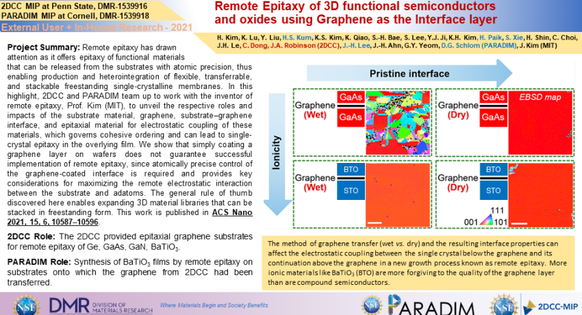
Remote Epitaxy of 3D functional semiconductors and oxides using Graphene as the Interface layer

Remote Epitaxy of 3D functional semiconductors and oxides using Graphene as the Interface layer

Project Summary: Remote epitaxy has drawn attention as it offers epitaxy of functional materials that can be released from the substrates with atomic precision, thus enabling production and heterointegration of flexible, transferrable, and stackable freestanding single-crystalline membranes. In this highlight, 2DCC and PARADIM team up to work with the inventor of remote epitaxy, Prof.

Orientation domain dispersions in wafer scale epitaxial monolayer WSe2 on sapphire

Orientation domain dispersions in wafer scale epitaxial monolayer WSe2 on sapphire

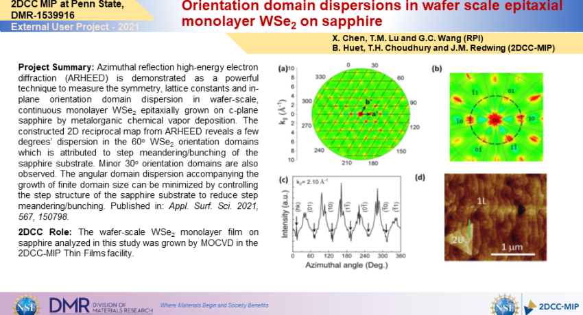
Project Summary: Azimuthal reflection high-energy electron diffraction (ARHEED) is demonstrated as a powerful technique to measure the symmetry, lattice constants and in-plane orientation domain dispersion in wafer-scale, continuous monolayer WSe2 epitaxially grown on c-plane sapphire by metalorganic chemical vapor deposition.

NMR determination of Van Hove singularity and Lifshitz transitions in the nodal-line semimetal ZrSiTe

NMR determination of Van Hove singularity and Lifshitz transitions in the nodal-line semimetal ZrSiTe

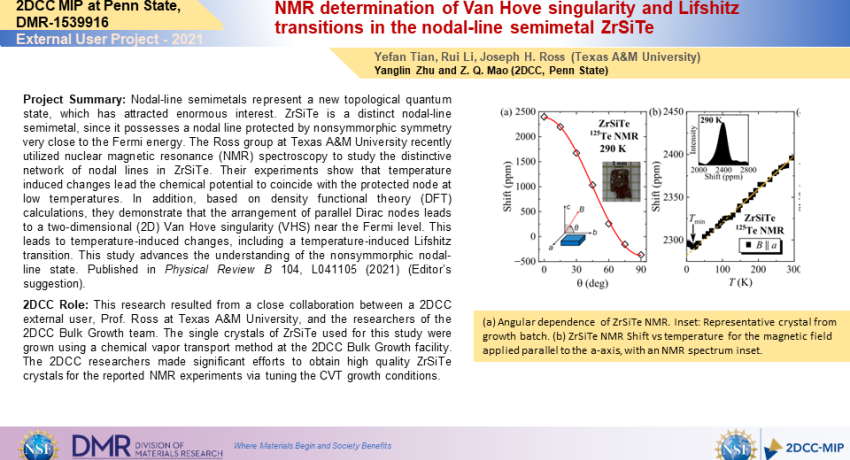
Project Summary: Nodal-line semimetals represent a new topological quantum state, which has attracted enormous interest. ZrSiTe is a distinct nodal-line semimetal, since it possesses a nodal line protected by nonsymmorphic symmetry very close to the Fermi energy. The Ross group at Texas A&M University recently utilized nuclear magnetic resonance (NMR) spectroscopy to study the distinctive network of nodal lines in ZrSiTe. Their experiments show that temperature induced changes lead the chemical potential to coincide with the protected node at low temperatures.

Modeling 2D Materials Growth Across Scales: Closing the MGI Loop

Modeling 2D Materials Growth Across Scales: Closing the MGI Loop

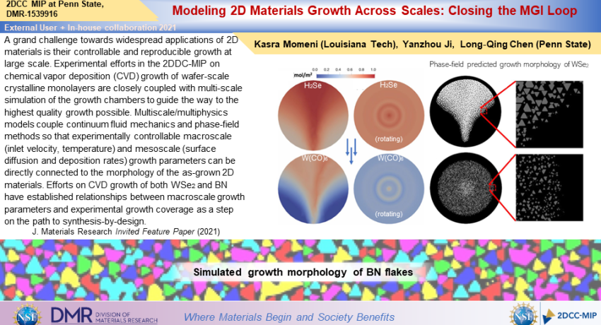
What Has Been Achieved: Multiscale/multiphysics models that couple continuum fluid mechanics and phase-field methods provide a means to map out how experimentally controllable macroscale (inlet velocity, temperature) and mesoscale (surface diffusion and deposition rates) parameters control the morphology of 2D materials, within the precise experimental growth geometries of the 2DCC, in a manner tha