Shrinking materials hold big potential for smart devices, researchers say

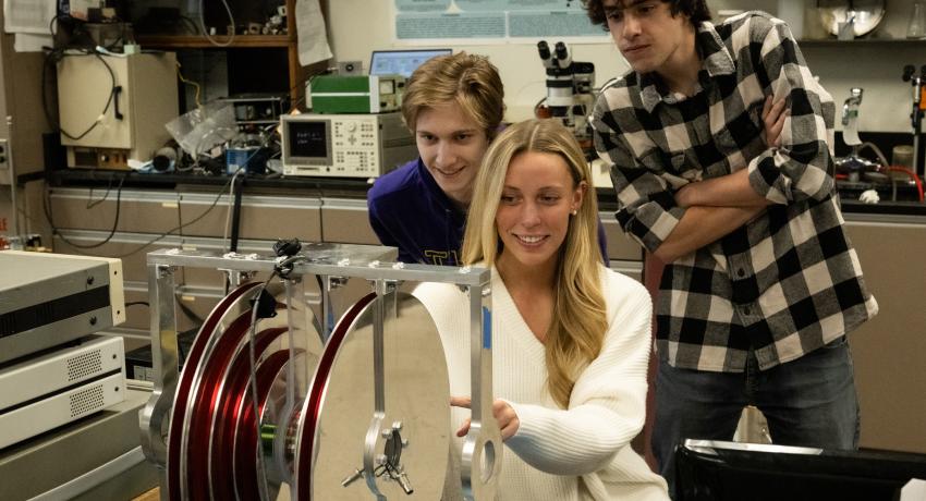
Wearable device ring tested in lab

Wearable electronics could be more wearable, according to a research team at Penn State. The researchers developed a scalable, versatile approach to designing and fabricating wireless, internet-enabled electronic systems that can better adapt to 3D surfaces, like the human body or common household items, paving the path for more precise health monitoring or household automation, such as a smart recliner that can monitor and correct poor sitting habits to improve circulation and prevent long-term problems.

Old-school material could power quantum computing, cut data center energy use

UNIVERSITY PARK, Pa. — A new twist on a classic material could advance quantum computing and make modern data centers more energy efficient, according to a team led by researchers at Penn State.   

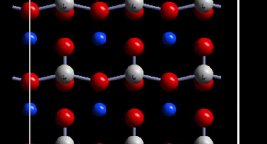
Barium titanate, first discovered in 1941, is known for its powerful electro-optic properties in bulk, or three-dimensional, crystals. Electro-optic materials like barium titanate act as bridges between electricity and light, converting signals carried by electrons into signals carried by photons, or particles of light.  

Seeing like a butterfly: Optical invention enhances camera capabilities

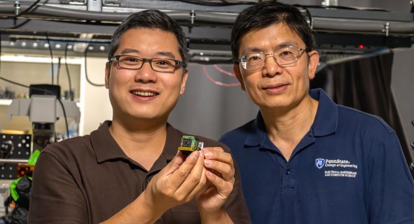
Two men holding a camera sensor

Butterflies can see more of the world than humans, including more colors and the field oscillation direction, or polarization, of light. This special ability enables them to navigate with precision, forage for food and communicate with one another. Other species, like the mantis shrimp, can sense an even wider spectrum of light, as well as the circular polarization, or spinning states, of light waves. They use this capability to signal a “love code,” which helps them find and be discovered by mates.

Q&A: How can advanced chip packaging help redesign the future of semiconductors?

Microchips Image

Researchers explain how chip architecture and Penn State-led initiatives can help jump-start U.S. chip manufacturing

By Tim Schley

The phrase “advanced chip packaging” might conjure images of a fancy Pringles can. For those who manufacture semiconductors — also known as integrated circuits, chips or microchips — it represents a new frontier, a race to design and mass produce the next generation of semiconductors that use less energy while delivering more computing power.

Solution found to problem bedeviling semiconductor researchers

Sapphire substrates

By Jamie Oberdick

Researchers from the National Science Foundation-sponsored Two-Dimensional Crystal Consortium (2DCC-MIP) - Materials Innovation Platform may have come up with a solution for a bottleneck that has confounded researchers trying to develop high-quality 2D semiconductors for next generation electronics such as Internet of Things (IoT) and artificial intelligence.