

The Nanofabrication lab owns two Zeiss FESEMs (field emission scanning electron microscopy), Merlin and Gemini 500. Both can image features down to 1 nm resolution. FESEM stage can handle samples from small pieces up to 8” wafer. The maximum sample height can be 2” tall. Both FESEMs are equipped with 3” loadlocks. It takes only 1-2 minutes to transfer in and out when the sample is less than 3” in size.
Gemini 500 Instrument DOI: 10.60551/s8kd-hc72
Merlin Instrument DOI: 10.60551/6cg4-rx71
Zeiss FESEM is known for its excellent usability and very easy to learn. It has excellent low KV resolution, and sees no difference when imaging conductive materials, magnetic materials, and cross sectional samples due to its unique design of Gemini column (in-column beam deacceleration, electrostatic final lens, etc).
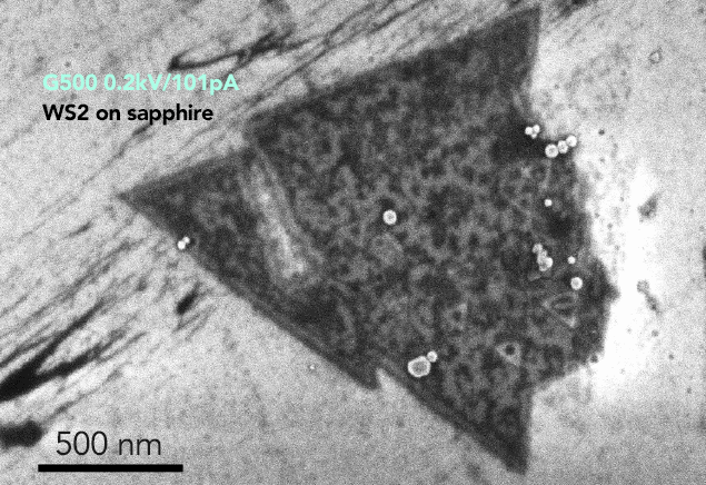
Zeiss improved the design of Gemini I column on G500 FESEM by adding an additional lens at the end of the column which can resolve 1 nm feature at 0.5KV. Therefore, G500 is designed for imaging 2D materials. It is also equipped with VP (vat photopolymerization) and nanoVP imaging modes, offering additional ways to leverage when imaging insulating materials.
Other than imaging, Merlin is also configured for EDS (energy dispersive spectroscopy) measurement with Oxford UltimMax 100 sensor. Merlin is equipped with Gemini II column, which allows user to change beam current continuously between 10pA and 300nA without compromising resolution significantly, making switching between high resolution imaging and EDS analysis an ease.
WS2 on sapphire. Image: 2DCC-MIP Joan Redwing Group / Penn State
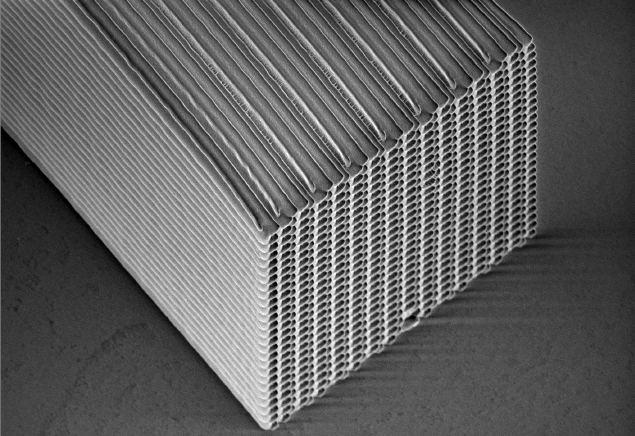
3D printed structure. Image: Jiho Noh, Physics / Penn State
- Loadlock sample transfer (sample loading/unloading less than 2 min)
- Large samples (upto 8” wide, 2” tall)
- Great in imaging insulating, magnetic, and cross sectional samples
- In-situ sample cleaning
- Low voltage high resolution imaging (excellent for 2D materials)
- Insulating material imaging (quartz, sapphire, glass, fiber, etc.)
- Cross-sectional view imaging
- BSE imaging
- Cathodoluminescence imaging
- EDS analysis