Solution found to problem bedeviling semiconductor researchers

Sapphire substrates

By Jamie Oberdick

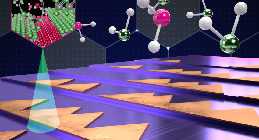
Researchers from the National Science Foundation-sponsored Two-Dimensional Crystal Consortium (2DCC-MIP) - Materials Innovation Platform may have come up with a solution for a bottleneck that has confounded researchers trying to develop high-quality 2D semiconductors for next generation electronics such as Internet of Things (IoT) and artificial intelligence.  

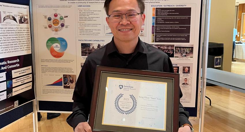
Seng Huat (Sam) Lee

Seng Huat (Sam) Lee

Assistant Research Professor - Bulk Crystal Growth

(e) shl12@psu.edu 
(o) 573-647-1436
N-315 Millennium Science Complex

Chen Chen

Chen Chen

Assistant Research Professor - Thin Films, MOCVD, Raman/PL

(e) cuc33@psu.edu
N-301 Millennium Science Complex

New type of semiconductor may advance low-energy electronics

By Jamie Oberdick

A research partnership between Penn State and the Massachusetts Institute of Technology (MIT) could enable an improved method to make a new type of semiconductor that is a few atoms thin and interacts with light in an unusual way. This new semiconductor could lead to new computing and communications technologies that use lower amounts of energy than current electronics.