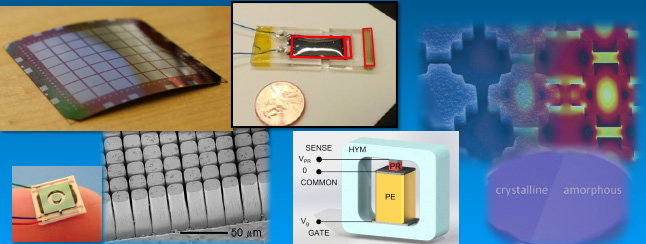
The Trolier-McKinstry group research primarily revolves around thin film dielectric and piezoelectric materials. The group works both to probe the fundamental mechanisms that control the magnitude of the achievable properties and to integrate new materials into devices.
Thin film piezoelectrics offer a number of advantages in microelectromechanical systems (MEMS), due to the large motions that can be generated, often with low hysteresis, the high available energy densities, as well as high sensitivity sensors with wide dynamic ranges, and low power requirements. The Trolier-McKinstry group has explored a wide range of perovskite thin films for these applications, and has developed new characterization tools for measurement of thin film piezoelectric properties. Of particular interest is the development of high actuation authority films which are CMOS compatible both in terms of the required drive voltages and the processing temperatures. Patterning approaches, including reactive ion etching, and microcontact printing, are also being explored. A wide variety of piezoelectric MEMS devices have been fabricated, including accelerometers, rf switches, medical ultrasound transducers, pump actuators, and adaptive optics systems. Lead zirconate titanate (PZT) and other specialty piezoelectric films are available from the group via the Penn State NNIN site.
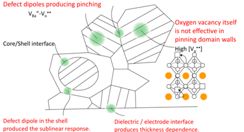
For both piezoelectric and dielectric materials, the group has been focusing on characterizing the role of domain wall motion in governing the observed electrical and electromechanical properties. In many materials, Rayleigh analysis can be employed to characterize the ac field dependence of the functional properties. The group has begun to unpick how different families of perturbations in the lattice influence the domain wall motion, as shown in the figure for the case of BaTiO3 capacitors through the use of a combination of local and global measurements. At higher field levels, first order polarization reversal curves are used to assess the field dependence of the properties.
In addition, we have developed new families of tunable dielectric materials, where the permittivity can be changed by the application of a dc bias field. The group was the first to demonstrate that Bi1.5ZnxNb1.5O6+x (where x = 0.5 to 1) provide reasonable tunability (~50%) coupled with excellent temperature stability and low losses. Subsequently, it was shown that pulsed laser crystallization can be used to decrease the processing temperatures to 400°C, enabling integration onto polyimide.
Finally, in the area of bulk piezoelectric materials, the Messing and Trolier-McKinstry groups have worked to develop the process of templated grain growth to develop high levels of crystallographic texture. Because many piezoelectric materials are strongly anisotropic in either their polarization or their polarizability, use of appropriately oriented single crystals can maximize the achievable piezoelectric response. Unfortunately, growth of large single crystals in multicomponent oxides is often difficult, and the resulting materials are too expensive for use in some applications. Oriented polycrystalline ceramics offer a useful compromise, as they can be prepared using ceramic processing approaches, and offer properties intermediate between those of single crystals and randomly oriented polycrystalline samples.
In addition, we have developed new families of tunable dielectric materials, where the permittivity can be changed by the application of a dc bias field. The group was the first to demonstrate that Bi1.5ZnxNb1.5O6+x (where x = 0.5 to 1) provide reasonable tunability (~50%) coupled with excellent temperature stability and low losses. Subsequently, it was shown that pulsed laser crystallization can be used to decrease the processing temperatures to 400°C, enabling integration onto polyimide.