
Advanced EBL Process Calibration Capability Under Development with GenISys
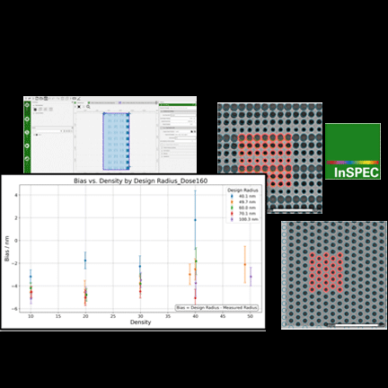
The Nanofab is actively developing enhanced electron beam lithography capabilities in collaboration with GenISys, focusing on their Inspec inspection software for automated process calibration and optimization. Inspec is an advanced integrated SEM metrology and inspection solution that upgrades a standard SEM into a dedicated tool for sophisticated pattern driven automated measurements while maintaining versatility, significantly increasing SEM utilization and productivity through improved data quality and consistency. Chad Eichfeld recently presented at the GenISys beam meeting during the EIPBN conference in Savannah, Georgia, showcasing the software's powerful ability to calibrate electron beam lithography processes through automated Inspec measurements with direct export functionality to Tracer calibration software and subsequently to Beamer pattern preparation software. This seamless integration creates a streamlined feedback loop that enables users to rapidly adjust lithographic patterns and continuously monitor process performance, significantly reducing the time and manual effort typically required for EBL optimization. The automated measurement and export capabilities promise to transform how researchers approach pattern fidelity and process control, offering unprecedented precision and efficiency in electron beam lithography workflows. This software is currently available to users and is perfectly matched with our Zeiss Crossbeam 550L, which features a 200mm capable stage with submicron stage repeatability, providing the precision platform necessary for accurate automated measurements and reliable process feedback. Researchers interested in utilizing this capability can contact Chad Eichfeld or Bangzhi Liu.
New Eshylon Charging Station and Carrier Wafers Now Available in Nanofab
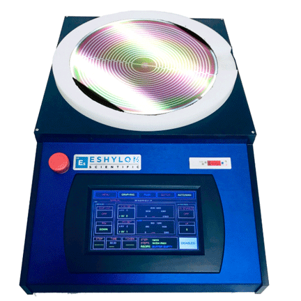
The Nanofab has recently added the innovative Eshylon Charging Station and Carrier wafers to enhance capabilities for mounting thin wafers and small parts in etch tools. This electrostatic carrier system offers significant advantages over traditional thermal tape methods, including superior temperature stability during high-temperature processes, elimination of adhesive residue that can contaminate samples, improved uniformity of substrate contact and heat transfer, and the ability to handle extremely thin or fragile substrates without mechanical stress or damage. The electrostatic holding force provides consistent, reliable securing of parts throughout the entire etch process while maintaining excellent thermal conductivity. Researchers interested in exploring how these carrier wafers could benefit their specific applications are encouraged to contact Guy Lavallee to discuss implementation and optimize their processing protocols.