Team Research Project #1: p-type 2D Field Effect Transistors
Objective: Develop high-performance p-type 2D field effect transistors (FETs) based on WSe2 for integrated circuits.
Approach: Grow WSe2 films via metal organic chemical vapor deposition (MOCVD), investigate p-type doping techniques, and nanofabricate devices for testing. Explore alternate pathways for surface charge transport doping.
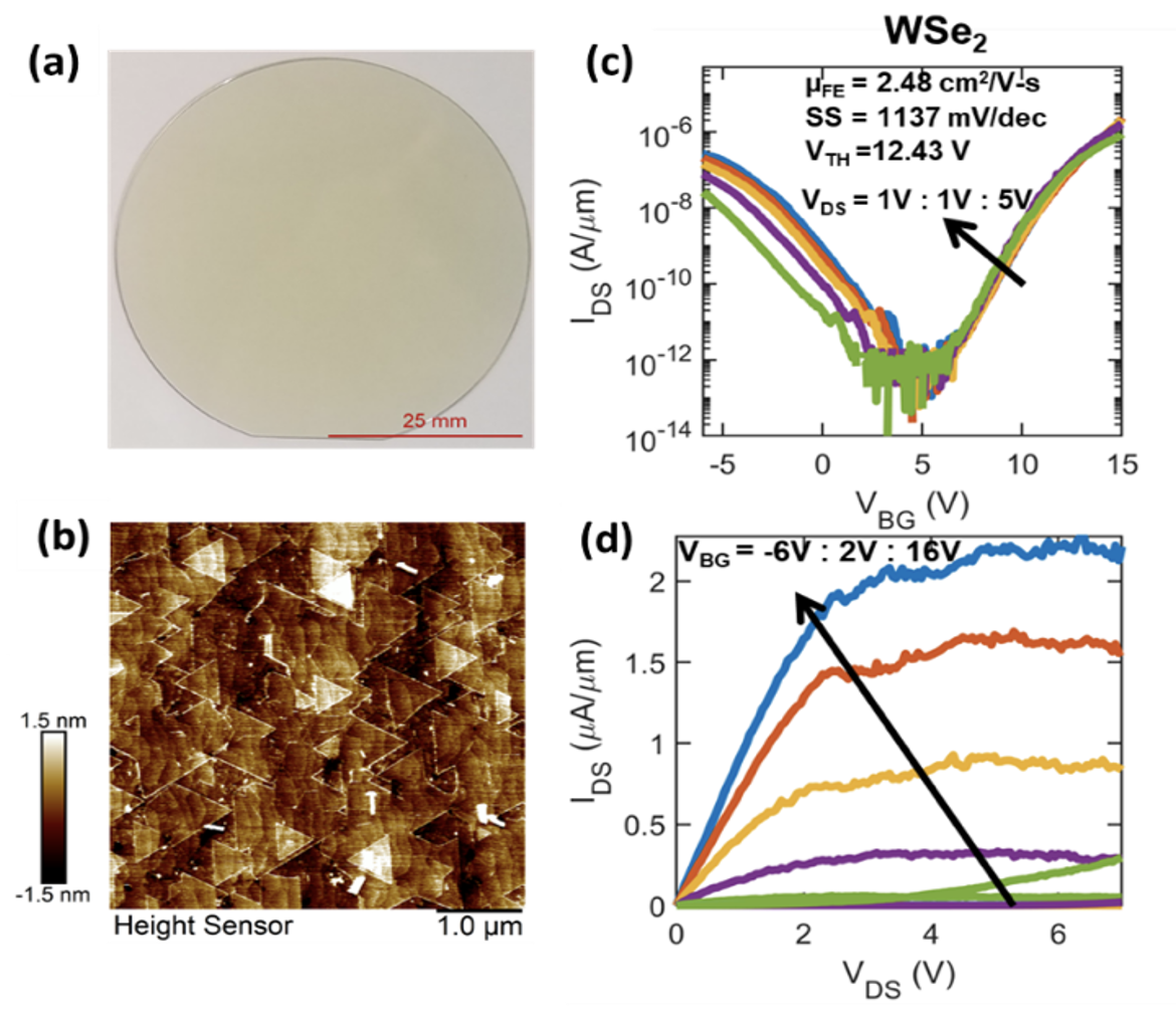 |
| (a) WSe2 grown by MOCVD on 2” sapphire. (b) AFM of coalesced WSe2 films. (c) Ambipolar transfer characteristics of WSe2 FET and (d) drain-source current vs. drain-source voltage. |
Potential Student Research Projects:
• Grow WSe2 films via MOCVD.
• Investigate techniques for p-type doping of WSe2.
• Nanofabricate devices for testing.
• Perform atomic layer deposition (ALD) for surface charge transport doping.
• Test FET devices and analyze data.
Team Research Project #2: Biosensing and Bioelectronic Devices Based on 2D Materials
Objective: Develop biosensors using 2D materials with in-situ tunability for selective and amplified sensing.
Applications: Detection of biomarkers in sweat, saliva, bacterial, and cancer cells.
Materials: CVD-grown 2D materials and mechanically exfoliated 2D heterostructures.
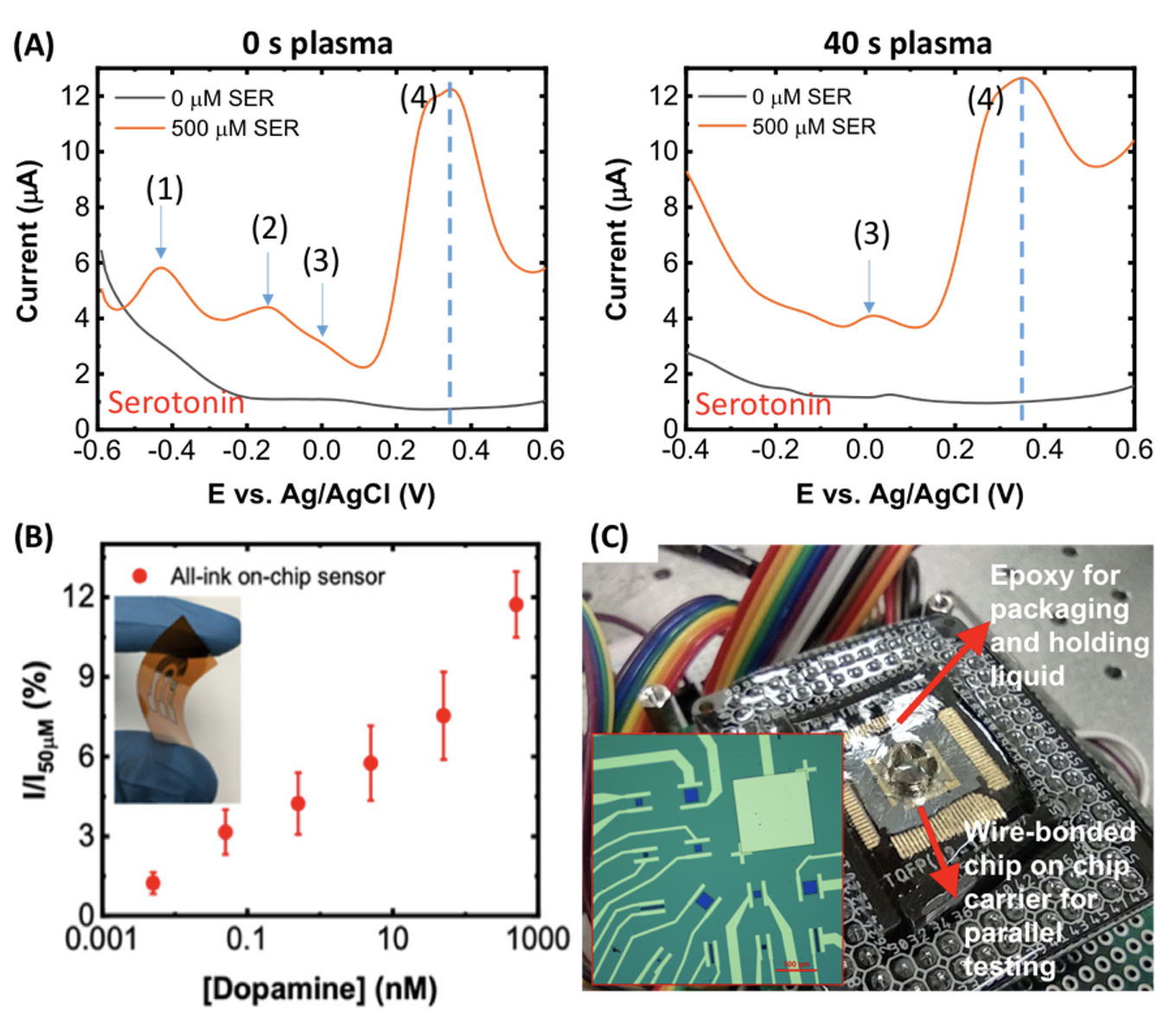 |
| (a) Graphene response to serotonin without and with 40 s plasma. With plasma, quenching of peaks 1 and 2 is observed with no effect on peaks 3 and 4. (b) Detection of dopamine down to few pM using a post-deposition treatment of a screen-printed graphene sensor. (c) Image of packaged device.* |
Potential Student Research Projects:
• Benchmark process-property-performance of devices based on CVD-grown 2D materials.
• Prepare mechanically exfoliated 2D heterostructures.
• Investigate dual gating effects on electrochemical response.
• Study the impact of plasma treatment on sensor properties.
• Explore screen-printed devices based on 2D inks.
• Contribute to the fabrication and characterization of biosensors.
Team Research Project #3: Topological Semimetals for Terahertz Optical Modulators
Objective: Characterize optical properties of topological semimetals for THz applications, including modulators and waveguides.
Materials: Thin films of topological semimetals (chalcogenides and intermetallics).
Methods: Retrieve THz optical constants, use lithographic techniques to pattern thin films for nonreciprocal plasmon excitations. Benchmark materials as optical modulators.
Potential Student Research Projects:
1. Synthesize thin films of topological semimetals.
2. Retrieve THz optical constants using FTIR spectroscopy and modeling.
3. Use lithographic techniques to pattern thin films for nonreciprocal plasmon excitations.
4. Benchmark materials as optical modulators.
5. Contribute to the characterization of optical properties.
Team Research Project #4: Single-Crystal Topological Semimetals for Electrical Interconnects
Objective: Explore topological semimetals for low-resistivity electrical interconnects between transistors.
Significance: Increase operating frequency of integrated circuits.
Approach: Prepare intermetallic semimetals using co-sputtering and annealing, utilize single-crystal MoS2 films as substrates, and characterize synthesized layers. Measure current transport.
|
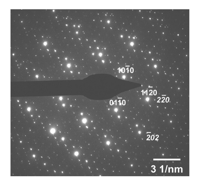
| Epitaxial Cu on single-crystal MoS2.$ |
Potential Student Research Projects:
• Prepare intermetallic semimetals using co-sputtering or annealing.
• Utilize single-crystal MoS2 films as substrates for crystallization.
• Prepare films with different nanoscale thicknesses.
• Identify synthesized phases using diffraction techniques.
• Measure resistance at room temperature and as a function of temperature and magnetic field.
Team Research Project #5: On-chip Machine Vision Platform for Image Classification
Objective: Improve 2D materials-based phototransistors and develop a low-power on-chip vision platform for image classification.
Significance: Address energy consumption challenges in conventional machine vision systems.
Approach: Optimize transfer process for MoS2 films, mitigate polymer residues, and explore ideal contact metals. Develop a high-performance 2D vision platform using phototransistors.
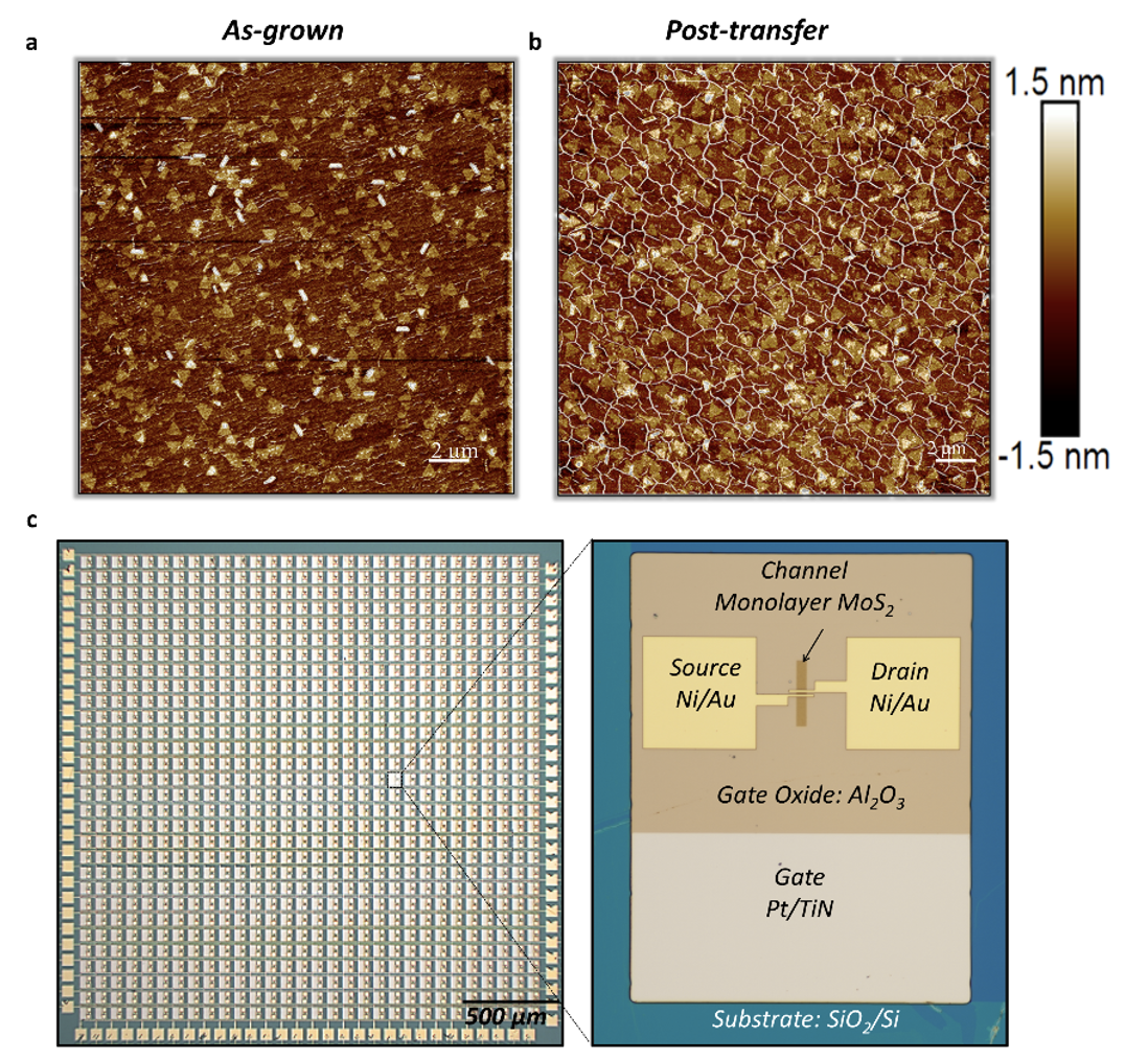
|
| AFM images of (a) as-grown and (b) post-transfer MoS2. (c) Optical image of 900-pixel machine vision platform in a cross-bar architecture and corresponding optical image of individual MoS2 phototransistor. |
Potential Student Research Projects:
1. Optimize transfer process for MoS2 films.
2. Mitigate polymer residues in transferred films.
3. Fabricate devices using transferred MoS2.
4. Prepare different contact metals and explore their impact.
5. Contribute to device characterization.
6. Train target images in the vision platform using photogating.