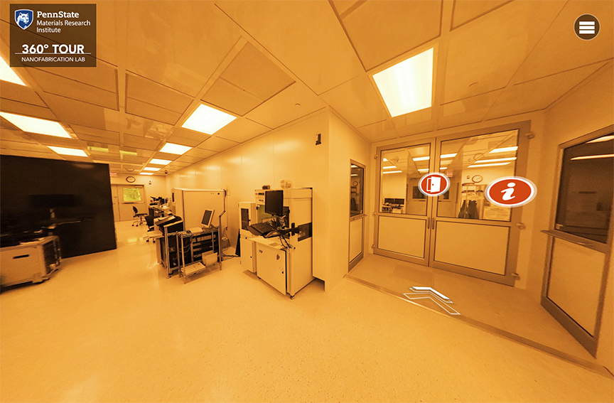


The Penn State Nanofabrication Laboratory saves companies the expense of maintaining their own state-of-the-art equipment and provides a highly skilled technical staff dedicated to working with companies in Pennsylvania and world wide.
Innovation at the Nanoscale
At Penn State, nearly one hundred research groups are engaged in high-impact science and engineering at the nanoscale. The Nanofab provides specialized instruments and experienced, highly trained technical staff who support researchers in areas that reflect our faculty strengths, including sputter deposition, atomic layer deposition, thin film piezoelectrics, two-dimensional materials, CMOS and MEMs.
Technical capabilities that set the Nanofab apart include e-beam lithography of nanoscale features on curved surfaces and the ability to integrate non-traditional electronic materials, such as complex oxides, chalcogenides, graphene etc., into complex structures. The laboratory has world-class capabilities in the area of deposition, etch, lithography and material modification.