Q&A: How can advanced chip packaging help redesign the future of semiconductors?

Microchips Image

Researchers explain how chip architecture and Penn State-led initiatives can help jump-start U.S. chip manufacturing

By Tim Schley

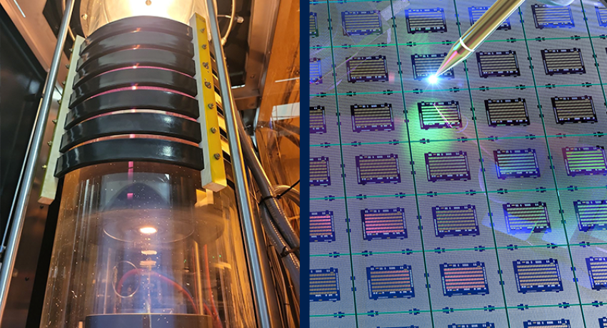
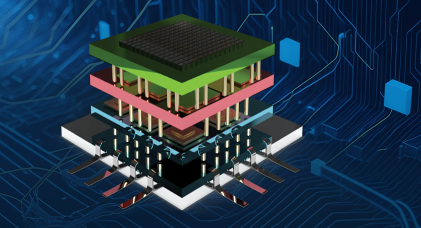
The phrase “advanced chip packaging” might conjure images of a fancy Pringles can. For those who manufacture semiconductors — also known as integrated circuits, chips or microchips — it represents a new frontier, a race to design and mass produce the next generation of semiconductors that use less energy while delivering more computing power.

‘Surprising’ hidden activity of semiconductor material spotted by researchers

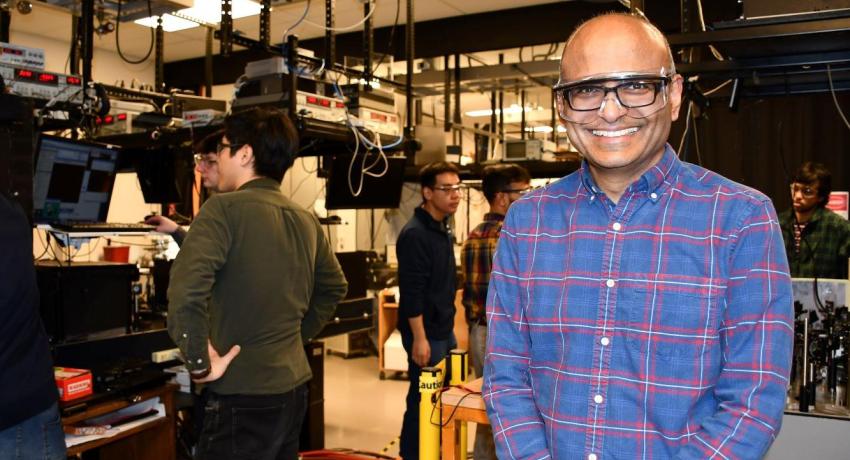
Prof. Gopalan in lab with students

By Jamie Oberdick

New research suggests that materials commonly overlooked in computer chip design actually play an important role in information processing, a discovery which could lead to faster and more efficient electronics. Using advanced imaging techniques, an international team led by Penn State researchers found that the material that a semiconductor chip device is built on, called the substrate, responds to changes in electricity much like the semiconductor on top of it.

Silicon Carbide Innovation Alliance to drive industrial-scale semiconductor work

SCIA News Graphic

By Jamie Oberdick

Known for its ability to withstand extreme environments and high voltages, silicon carbide (SiC) is a semiconducting material made up of silicon and carbon atoms arranged into crystals that is increasingly becoming essential to modern technologies like electric vehicles, renewable energy systems, telecommunications infrastructure and microelectronics.  

Integrating dimensions to get more out of Moore’s Law and advance electronics

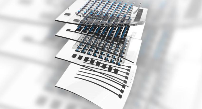
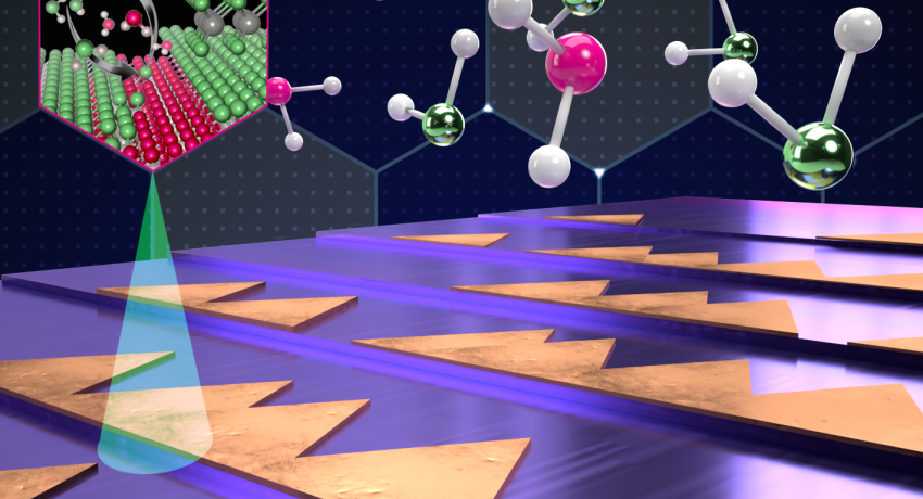
Diagram image of 2D layered advanced electronics

By Jamie Oberdick and Ashley WennersHerron

Moore's Law, a fundamental scaling principle for electronic devices, forecasts that the number of transistors on a chip will double every two years, ensuring more computing power — but a limit exists.

Today's most advanced chips house nearly 50 billion transistors within a space no larger than your thumbnail. The task of cramming even more transistors into that confined area has become more and more difficult, according to Penn State researchers.

Solution found to problem bedeviling semiconductor researchers

Sapphire substrates

By Jamie Oberdick

Researchers from the National Science Foundation-sponsored Two-Dimensional Crystal Consortium (2DCC-MIP) - Materials Innovation Platform may have come up with a solution for a bottleneck that has confounded researchers trying to develop high-quality 2D semiconductors for next generation electronics such as Internet of Things (IoT) and artificial intelligence.